Semiconductor structures and methods of forming them

A technology of semiconductor and nanostructure, applied in semiconductor devices, semiconductor/solid-state device manufacturing, transistors, etc., can solve problems such as short channel effect, leakage current power consumption increase, chip integration limit, etc., and achieve high carrier migration Efficiency, improved performance, and improved contact area

Active Publication Date: 2018-07-10
SEMICON MFG INT (SHANGHAI) CORP
View PDF3 Cites 0 Cited by
  • Summary
  • Abstract
  • Description
  • Claims
  • Application Information

AI Technical Summary

Problems solved by technology

However, as the size of semiconductor devices continues to shrink, problems such as short channel effects, leakage currents, and increased power consumption become more and more significant. At the same time, more challenges are faced in device structures and manufacturing processes.
As a result, further improvement of chip integration is subject to more restrictions

Method used


Image

  • Semiconductor structures and methods of forming them
  • Semiconductor structures and methods of forming them
  • Semiconductor structures and methods of forming them

Examples


Embodiment Construction

[0033] As mentioned in the background technology, in the prior art, as the size of semiconductor devices is gradually reduced, various adverse effects restrict the further reduction of device size. How to use high-performance one-dimensional nanostructures to form transistors with better performance is an urgent problem to be solved. The problem.

[0034] This embodiment provides a method for forming transistors and complementary transistors using one-dimensional nanostructures to form transistors with higher performance and higher integration.

[0035]In order to make the above objects, features and advantages of the present invention more comprehensible, specific embodiments of the present invention will be described in detail below in conjunction with the accompanying drawings.

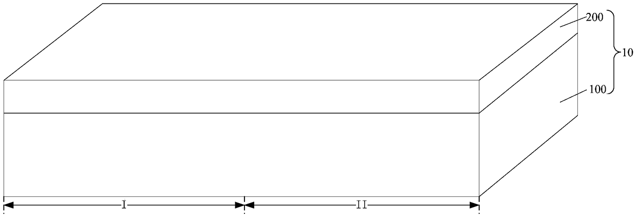
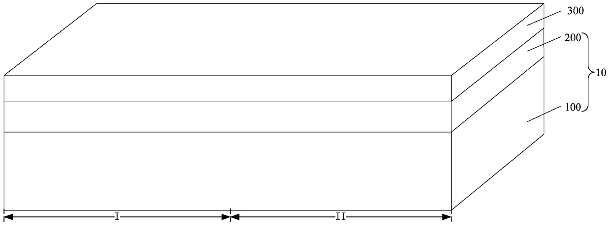
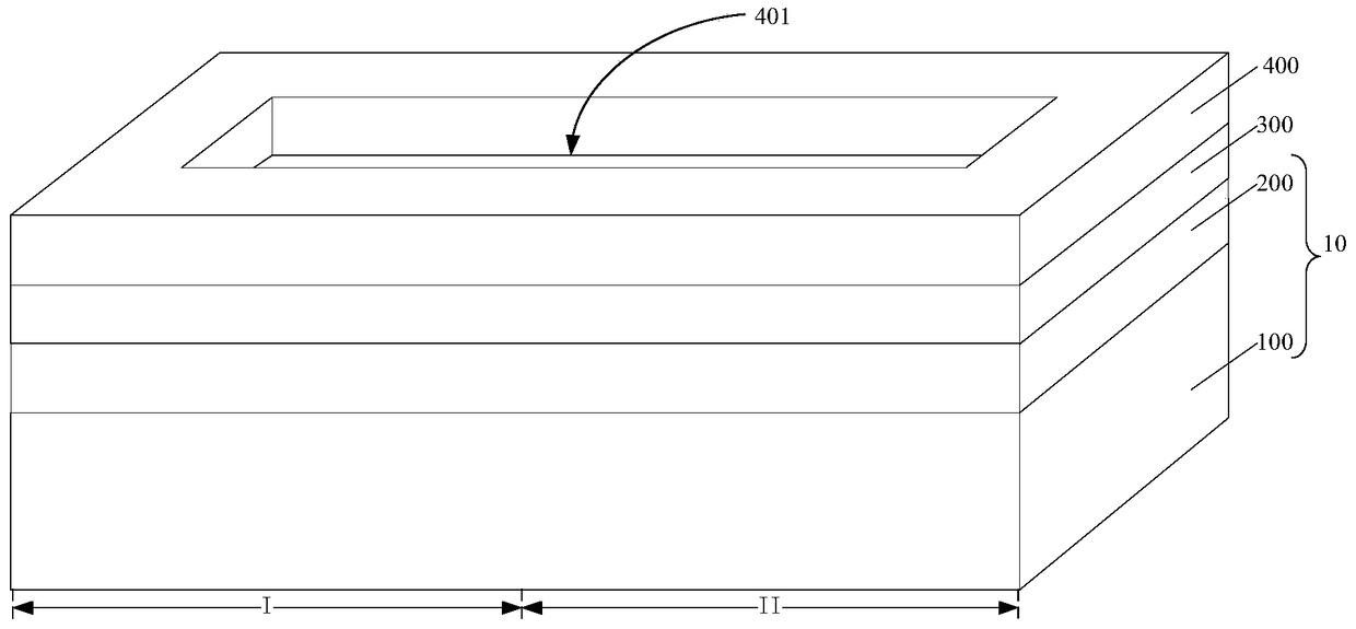
[0036] Please refer to figure 1 , providing a substrate 10 .

[0037] The material of the substrate 10 includes semiconductor materials such as silicon, germanium, silicon germanium, gallium ars...


PUM


Abstract

A semiconductor structure and its forming method, the forming method of the semiconductor structure comprising: providing a substrate, the substrate has a first region; forming a sacrificial layer on the surface of the substrate; forming a one-dimensional layer on the surface of the sacrificial layer nanostructure; removing part of the sacrificial layer, leaving the middle part of the one-dimensional nanostructure suspended, and the two ends of the one-dimensional nanostructure are located on the surface of the remaining sacrificial layer; part of the surface of the one-dimensional nanostructure on the first region is formed to surround the A first gate structure of the one-dimensional nanostructure; a first source contact layer and a first drain contact layer are formed on the one-dimensional nanostructure on the first regions on both sides of the first gate structure. The method can form transistors with higher performance and integration.

Description

technical field [0001] The invention relates to the technical field of semiconductors, in particular to a semiconductor structure and a forming method thereof. Background technique [0002] With the continuous development of semiconductor technology, high integration, multi-function and low power consumption are the main goals pursued by semiconductor devices. The size of semiconductor devices continues to shrink with the development of technology, making chips more and more integrated. However, as the size of semiconductor devices continues to shrink, problems such as short channel effects, leakage currents, and increased power consumption become more and more significant. At the same time, more challenges are faced in device structures and manufacturing processes. As a result, further improvement of chip integration is subject to more restrictions. [0003] In the prior art, the above-mentioned problems can be solved or alleviated to a certain extent by changing the chan...

Claims


Application Information

Patent Timeline
Patent Type & Authority Patents(China)
IPC IPC(8): H01L21/8238H01L21/336H01L27/092H01L29/06H01L29/78
Inventor 肖德元
Owner SEMICON MFG INT (SHANGHAI) CORP
Why Eureka
Try Eureka