A Miniaturized Stripline Power Amplifying Module

A technology of power amplification module and strip line, which is applied in the structural connection of printed circuits, printed circuit components, electrical components, etc., can solve the problems of cumbersome process steps, high manufacturing costs, unfavorable debugging, etc., and achieve superior quality and performance, The effect of simplifying the production process and saving the time required to make the copper skin

Active Publication Date: 2018-05-22
CHENGDU JINJIANG ELECTRONICS SYST ENG
View PDF6 Cites 0 Cited by
  • Summary
  • Abstract
  • Description
  • Claims
  • Application Information

AI Technical Summary

Problems solved by technology

However, the process steps of copper cladding are very cumbersome, the manufacturing cost is high, the operation takes a long time, it is easy to damage, it is not conducive to debugging, and it is not easy to realize at high frequency

Method used


Image

  • A Miniaturized Stripline Power Amplifying Module
  • A Miniaturized Stripline Power Amplifying Module
  • A Miniaturized Stripline Power Amplifying Module

Examples


specific Embodiment approach 1

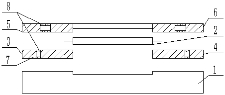
[0024] like figure 1 , Figure 5 and Image 6 As shown, a miniaturized stripline power amplification module, which includes a substrate 1 provided with a groove, a power transistor 2 installed in the groove, a printed board A3, a printed board B4, a printed board C5, a printed board Make board D6, feeder circuit A and feeder circuit B.

[0025] The printed board A3 and the printed board B4 are installed on the substrate 1, the printed board C5 cover is pressed on the printed board A3 and forms the input matching circuit of the power amplifier with the printed board A3; the printed board D6 cover is pressed on the printed board A3 The output matching circuit of the power amplifier is formed on the board B4 and the printed board B4; the input matching circuit is electrically connected to the input end of the power transistor 2, and the output matching circuit is electrically connected to the output end of the power transistor 2.

[0026] The feeding circuit A is arranged on t...

specific Embodiment approach 2

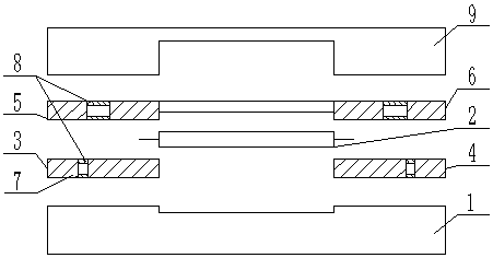
[0029] The difference between this specific embodiment and specific embodiment 1 is that: the printed board C5 and the printed board D6 are also provided with a metal cover 9, and the metal cover 9 is used to compress the upper and lower printed boards, Ensure close contact between upper and lower printed boards. The metal cover plate 9 has a hole at the DC blocking capacitor for installing the DC blocking capacitor. The specific structure is as figure 2 , Figure 5 and Image 6 shown.

specific Embodiment approach 3

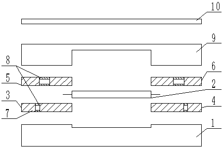
[0030] The difference between this specific embodiment and specific embodiment 2 is that the printed board C5 and the printed board D6 are manufactured separately, and the printed board E10, the feed circuit A and the feed circuit A are also provided on the metal cover 9 The circuits B are all arranged on the printed board E10, the feed circuit A is electrically connected to the input matching circuit, and the feed circuit B is electrically connected to the output matching circuit. The specific structure is as image 3 , Figure 5 and Figure 7 shown.


PUM


Abstract

The invention relates to a small strip-shaped linear power amplification module which comprises a substrate (1), a power transistor (2), a printing board A (3), a printing board B (4), a printing board C (5), a printing board D (6), a feed circuit A and a feed circuit B. The printing board C (5) and the printing board A (3) form an input matching circuit. The printing board D (6) and the printing board B (4) form an output matching circuit. The input matching circuit and the output matching circuit are connected with the power transistor (2). The feed circuit A and the feed circuit B are connected with the input matching circuit and the output matching circuit respectively. A gold-covered layer (7) and a copper-covered layer (8) are arranged on the side face and the combined face of each printing board respectively. Common grounding of a strip-shaped linear circuit in the module is achieved through copper-covered structures of the combined faces of the printing boards and gold-covered structures of the side faces of the printing boards, the number of procedures is reduced, a better common grounding effect is further provided, and large-power high-frequency work of the power amplification module is facilitated.

Description

technical field [0001] The invention relates to the technical field of power amplification modules, in particular to a miniaturized stripline power amplification module. Background technique [0002] Power amplifier modules not only play an important role in modern wireless communications, but also occupy an important position in military and civilian equipment. With the continuous development of semiconductor technology, the current power amplifier module is mainly realized by microstrip line. In the engineering manufacturing process, the stripline circuit is usually covered with copper skin to ensure the commonality between the upper printed board and the lower printed board. land. However, the process steps of copper cladding are very cumbersome, the manufacturing cost is high, the operation takes a long time, it is easy to be damaged, it is not conducive to debugging, and it is not easy to realize under high frequency. Contents of the invention [0003] The object of...

Claims


Application Information

Patent Timeline
Patent Type & Authority Patents(China)
IPC IPC(8): H05K1/02H05K1/14
CPCH05K1/0227H05K1/141H05K2201/049
Inventor 傅松
Owner CHENGDU JINJIANG ELECTRONICS SYST ENG
Why Eureka
Try Eureka