A dram DDR calibration circuit and method based on zq pins

A technology of DRAMDDRZQ and pins, which is applied in the field of detecting the use status of DRAMDDRZQ pins, can solve problems such as misjudgment, and achieve the effect of avoiding misjudgment and improving robustness

Active Publication Date: 2018-05-18
XI AN UNIIC SEMICON CO LTD
View PDF4 Cites 0 Cited by
  • Summary
  • Abstract
  • Description
  • Claims
  • Application Information

AI Technical Summary

Problems solved by technology

[0007] In order to solve the technical problem of misjudgment in the existing method for judging the use state of ZQ pins, the present invention provides a circuit and method for detecting the use state of ZQ pins of DRAM DDR

Method used


Image

  • A dram DDR calibration circuit and method based on zq pins
  • A dram DDR calibration circuit and method based on zq pins
  • A dram DDR calibration circuit and method based on zq pins

Examples


Embodiment 1

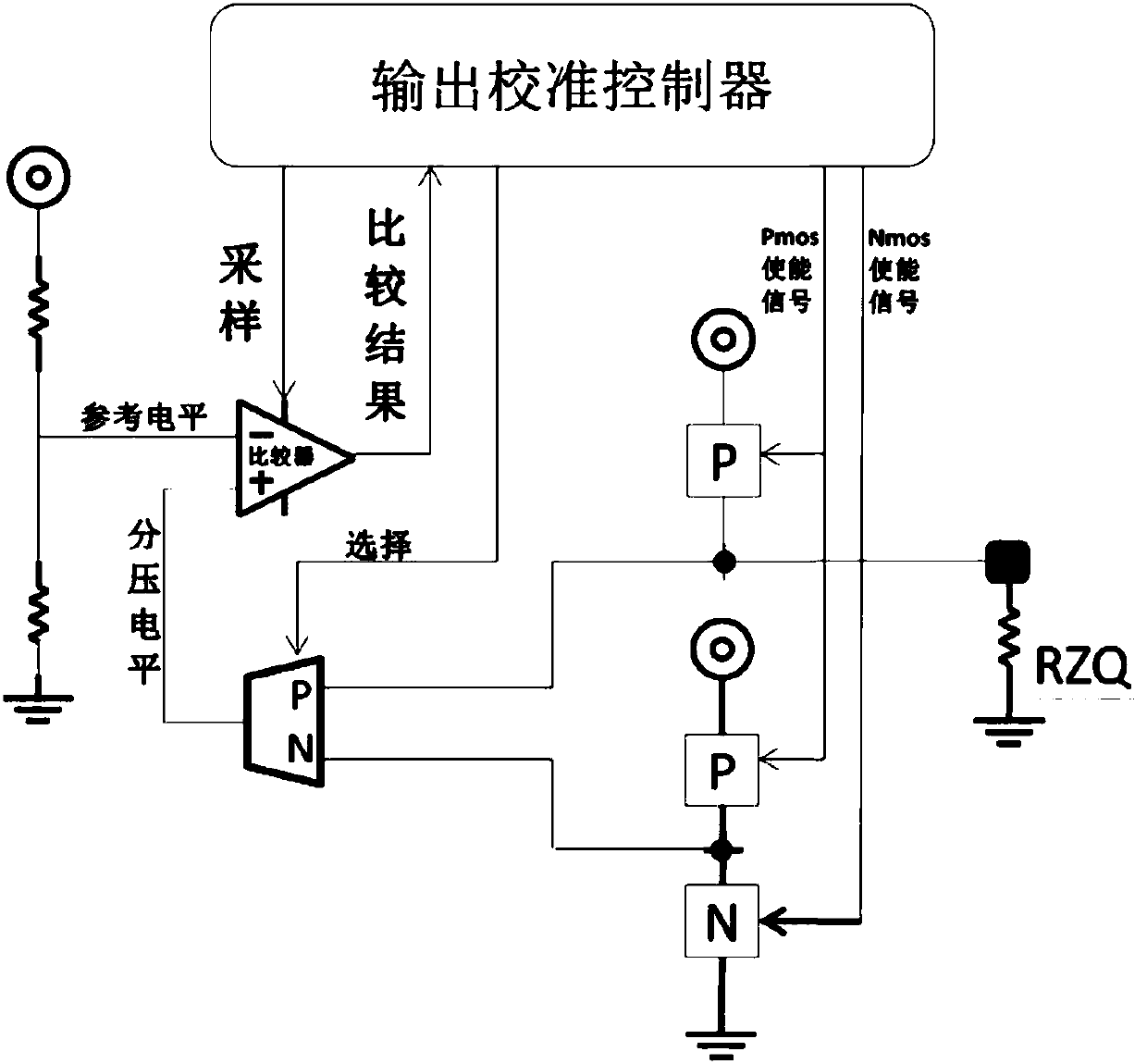
[0048] Embodiment 1: as Figure 4 As shown, the detection circuit of DRAM DDR ZQ pin usage status includes PMOS tube group, comparator, reference voltage supply circuit and ZQ pin judgment control module. The size of the PMOS tube is divided into N, so that the resistance of the PMOS tube group is at least 10 times greater than the reference resistance RZQ provided by the ZQ pin. The ZQ pin judgment control module includes a state judgment module. One end of the PMOS tube group is connected to the external power supply VDD. The other end of the PMOS tube group is connected to the ZQ pin and then connected to the positive phase input terminal of the comparator, the negative phase input terminal of the comparator is connected to the reference level, the output terminal of the comparator outputs the comparison result to the state judgment module, and the state judgment module Judge the use state of the ZQ pin according to the input comparison result.

[0049] Generally, the PMOS...

Embodiment 2

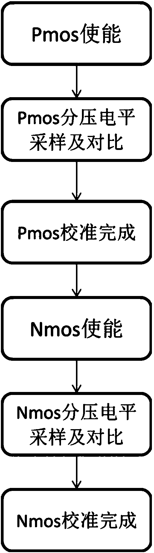
[0050] Embodiment 2: the detection method of DRAM DDR ZQ pin use state, comprises the following steps:

[0051] 1] Configure the PMOS enable signal so that the PMOS tube group is configured in the limit resistance state; for example, the limit resistance mode is configured as 2kΩ, and the general standard RZQ=240Ω;

[0052] 2] Compare the reference level and the divided voltage level to obtain the comparison result;

[0053] 3] According to the comparison result, judge the usage status of the ZQ pin:

[0054] If the divided voltage level is less than the reference level VDD / 2, the ZQ pin is valid and connected with a resistor RZQ;

[0055] If the divided voltage level is greater than the reference level VDD / 2, the ZQ pin is floating, and the resistor RZQ is not connected.

[0056] The working principle is to use 2kΩ to compare with the external standard RZQ=240Ω. If a ZQ resistor is connected, the divided voltage level must be much smaller than VDD / 2. If there is no external...

Embodiment 3

[0057] Embodiment 3: as Figure 5 As shown, the DRAM DDR calibration circuit includes a detection circuit, and also includes a mirrored PMOS tube group, an NMOS tube group, and a selector. The ZQ pin judgment control module also includes an enable generation module. The reference voltage generated by the reference voltage supply circuit is equal to VDD / 2, the PMOS tube with the smallest size in the PMOS tube group is divided into N, so that the resistance of the PMOS tube group is at least 10 times greater than the reference resistance RZQ provided by the ZQ pin, and the mirrored PMOS tube group is the same as the NMOS tube group and the PMOS tube group One end of the PMOS tube group is connected to the external power supply VDD, the other end of the PMOS tube group is connected to the ZQ pin and then connected to an input terminal of the selector; one end of the mirrored PMOS tube group is connected to the external power supply VDD, and the other end of the mirrored PMOS tube...


PUM


Abstract

The invention relates to a DRAM DDR calibration circuit and method based on a ZQ pin. The circuit comprises a PMOS transistor group, a comparator, a reference voltage providing circuit and a ZQ pin judgment control module. The reference voltage providing circuit generates reference voltage. N minimum size of PMOS transistors are formed in the PMOS transistor group through division so that the resistance value of the PMOS transistor group is enabled to be higher than reference resistance RZQ provided by the ZQ pin for 8-12 times. The ZQ pin judgment control module comprises a state judgment module. The PMOS transistor group is arranged between an external power supply VDD and the ZQ pin. The negative phase input end of the comparator is connected with reference level. The state judgment module judges the use state of the ZQ pin according to the comparison result. In order to solve the technical problems of misjudgment of an existing method for judging the use state of the ZQ pin, no hardware is additionally arranged in an existing ZQ pin use state calibration circuit, and no doubled area or power consumption is provided for wider comparison range.

Description

technical field [0001] The invention belongs to the field of DRAM DDR design, and in particular relates to a method for detecting the use state of DRAM DDR ZQ pins. Background technique [0002] Now the mainstream DRAM DDR has introduced the ZQ pin, and the ZQ pin is connected to an external resistor, the purpose of which is to provide a precise external reference resistor for the high-speed DRAM DDR. However, due to the fact that the update speed of many system platforms is slower than that of DRAM, it often appears that the new generation of high-speed DRAM DDR is used on the old system platform that has not been updated, and there are ZQ pins that are used on different generations of system platforms. different states. For example, the old system platform does not provide the definition of the ZQ pin, so there will be cases where the ZQ pin is floating. [0003] The existing internal design of DRAM DDR also considers such applications, so some solutions are provided. Th...

Claims


Application Information

Patent Timeline
Patent Type & Authority Patents(China)
IPC IPC(8): G01R31/00G01R31/02
CPCG01R31/00G01R31/50
Inventor 王嵩
Owner XI AN UNIIC SEMICON CO LTD
Why Eureka
Try Eureka