Positioning method for packaging and picking up chips

A positioning method and chip technology, which is applied to semiconductor/solid-state device parts, semiconductor devices, electrical components, etc., can solve problems such as picking up errors, and achieve the effect of avoiding picking up wrong chips and simple operation

Active Publication Date: 2016-03-02
唐山捷准芯测信息科技有限公司
View PDF4 Cites 6 Cited by
  • Summary
  • Abstract
  • Description
  • Claims
  • Application Information

AI Technical Summary

Problems solved by technology

However, there is a big hidden danger in using the chip map to identify and pick up the chip, which is the problem of wrong picking. How to realize the one-to-one correspondence between the chip map file and the physical wafer without making mistakes has become the primary problem to be solved when picking up the chip from the chip map file and packaging it.

Method used


Image

  • Positioning method for packaging and picking up chips
  • Positioning method for packaging and picking up chips

Examples


Embodiment Construction

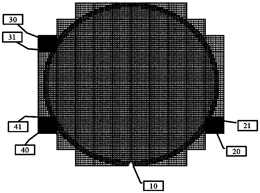
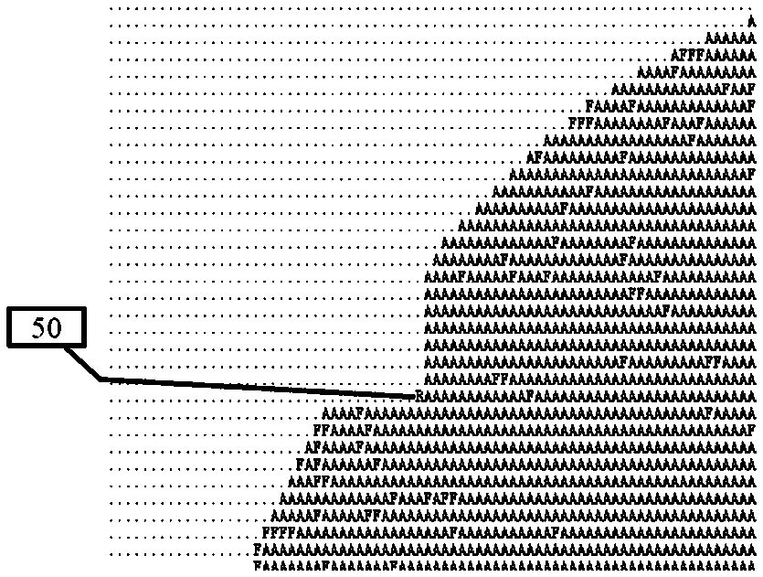
[0014] see figure 1 with figure 2 , the positioning method of the package pick-up chip of the present invention includes the modification of two parts, figure 1 Arrangement for the exposure area of ​​the actual wafer and its integrated circuit, where 10 is the positioning notch (Notch) of the wafer, and areas 20, 30, and 40 are the least exposed areas of effective chips on the edge; figure 2 It is a part of the wafer map (WaferMap) for the wafer test, and the positioning point 50 is the chip position of the wafer map corresponding to the physical positioning area.

[0015] see figure 1 with figure 2 , T2174 and other series of products based on the positioning method of the present invention have been mass-produced, and there are no errors in wafer manufacturing, wafer testing, and packaging and pick-up stages.

[0016] Adopt the positioning method of the integrated circuit production, testing and packaging of various embodiments of the present invention to pick up the ...


PUM


Abstract

The invention discloses a positioning method for packaging and picking up chips. The method comprises steps of: using triangular unexposed regions on the edge of a wafer as positioning regions in an integrated circuit production design process; in an integrated circuit chip manufacture process, selecting one or two of the triangular unexposed regions, not exposing or etching the one or two triangular unexposed regions, and selecting a positioning point in order to achieve pickup positioning; in an integrated circuit testing flow, bypassing the triangular unexposed regions, marking good or bad chips in wafer map file, and marking untested chips as invalid chips; and in an integrated circuit chip packing and picking process, picking up chips by using a wafer map and enabling positioning marks in the wafer map to correspond to special positioning patterns on entity wafers so that one-to-one correspondence between the wafer map file and the entity wafers is achieved and a problem of erroneously picking up a chip is prevented in a packaging process.

Description

technical field [0001] The invention relates to an integrated circuit manufacturing process and process, and the field of integrated circuit chip packaging, especially the field of integrated circuit packaging that adopts a positioning method to pick up chips. Background technique [0002] With the rapid development of integrated circuit technology, the chip size is getting smaller and smaller, and the number of chips produced by a single wafer is increasing. At the same time, due to the increase of chip functions and the increase of packaging pins, the packaging of integrated circuit chips is becoming more and more challenging, and the cost of packaging is increasing. Therefore, how to reduce the error rate in the packaging process becomes more and more difficult. As the process becomes more and more important, the step of picking up the chip die, which is the first step in chip packaging, becomes even more important. [0003] In the existing integrated circuit chip manufa...

Claims


Application Information

Patent Timeline
Patent Type & Authority Applications(China)
IPC IPC(8): H01L21/68H01L21/67H01L23/544
CPCH01L21/681H01L21/67271H01L21/67282H01L21/67294H01L23/544H01L2223/5444
Inventor 肖金磊欧阳睿刘静解辰
Owner 唐山捷准芯测信息科技有限公司
Why Eureka
Try Eureka