Bidirectional transient voltage suppression device

A transient voltage suppression and device technology, which is applied in the direction of electric solid devices, electrical components, semiconductor devices, etc., can solve the problems that the electrostatic protection ability of the device cannot be fully exerted, the failure of the ESD protection device, and the small discharge current of the device, etc., to achieve The effect of improving electrostatic discharge capacity, increasing maintenance voltage, and increasing device area

Active Publication Date: 2016-03-02
SUPERESD MICROELECTRONICS TECH CO LTD
View PDF3 Cites 18 Cited by
  • Summary
  • Abstract
  • Description
  • Claims
  • Application Information

AI Technical Summary

Problems solved by technology

However, interdigitated devices often cause premature failure of ESD protection devices due to uneven current discharge, and the potential electrostatic protection capabilities of the device are not fully utilized, resulting in a small discharge current per unit area of ​​the device

Method used


Image

  • Bidirectional transient voltage suppression device
  • Bidirectional transient voltage suppression device
  • Bidirectional transient voltage suppression device

Examples


Embodiment Construction

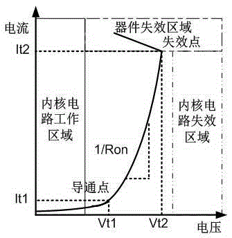
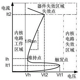
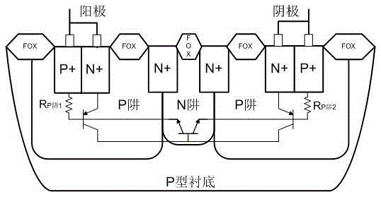
[0021] Such as Figure 5 As shown, the bidirectional transient voltage suppression device of the present invention includes five layers, wherein the bottom layer is a P-type substrate 100; the second layer is an N-type deep well 200 arranged on the P-type substrate 100; the third layer is formed on The first P well 301 and the second P well 302 on the N-type deep well 200; the fourth layer is the first N well 402 formed on the N-type deep well, and the second N well 401 formed in the P well 301, The third N well 403 formed in the P well 302; the fifth layer is six heavily doped regions: in the first P well 301, from left to right are the first P+ implantation region 501 and the first N+ implantation region 502 , the second N+ implantation region 503, wherein the second N+ implantation region 503 straddles the first P well 301 and the N well 401, and the left boundary of the second N+ implantation region 503 is flush with the left boundary of the second N well 401; the second P...


PUM


Abstract

The invention discloses an NPNPN-type bidirectional transient voltage suppression device which is based on a silicon planar process, has high maintaining voltage and high peak current, and is capable of bidirectionally clamping transient overvoltage. The NPNPN-type bidirectional transient voltage suppression device comprises a P-type substrate, wherein an N-type deep pit is arranged on the P-type substrate, a first P pit, a first N pit and a second P pit are arranged in the N-type deep pit, a first P+ injection region, a first N+ injection region, a second N pit and a second N+ injection region are sequentially arranged in the P pit from left to right, the second N+ injection region bridges the first P pit and the first N pit, a third N+ injection region, a third N pit, a fourth N+ injection region and a fifth P+ injection are sequentially arranged in the second P pit from left to right, the third N+ injection region bridges the second P pit and the first N pit, the first P+ injection region and the first N+ injection region are connected with a positive electrode, and the fourth N+ injection region and the second P+ injection region are connected to a negative electrode. The device can be used for transient overvoltage suppression on a chip pin with a signal level of (-5)V to (+5)V.

Description

technical field [0001] The invention relates to the field of integrated circuits, in particular to a bidirectional thyristor structure transient voltage suppression device based on silicon plane technology and applicable to -5V-+5V chip pins. Background technique [0002] In the electronics industry, static electricity is a key factor affecting the reliability of integrated circuits (Integrated Circuit, IC). The accumulation and discharge of static electricity is an inevitable phenomenon in all aspects of integrated circuit manufacturing, packaging, transportation, assembly and use. Static electricity is especially destructive in harsh environments such as handheld devices, outdoor applications, and extraterrestrial space. According to statistics, chip failures caused by Electro-Static Discharge (ESD) account for 38% of the total failures of integrated circuit products. Therefore, electrostatic protection has become an important aspect to be considered in the reliability d...

Claims


Application Information

Patent Timeline
Patent Type & Authority Applications(China)
IPC IPC(8): H01L27/02H01L29/06H01L29/74
CPCH01L27/0248H01L29/06H01L29/747
Inventor 汪洋董鹏金湘亮周子杰
Owner SUPERESD MICROELECTRONICS TECH CO LTD
Why Eureka
Try Eureka