
Microwave digital apparatus and processing method therefor

A digital device and microwave technology, applied in circuit devices, printed circuits, electrical components, etc., can solve the problems of high processing cost and low processing efficiency, and achieve the effects of low processing cost, high processing efficiency and reduced processing cost.

Active Publication Date: 2016-03-16
ANHUI SUN CREATE ELECTRONICS
View PDF5 Cites 1 Cited by
  • Summary
  • Abstract
  • Description
  • Claims
  • Application Information

AI Technical Summary

Problems solved by technology

High processing cost and low processing efficiency

Method used


Image

  • Microwave digital apparatus and processing method therefor
  • Microwave digital apparatus and processing method therefor
  • Microwave digital apparatus and processing method therefor

Examples


Embodiment Construction

[0043] The structural features of the present invention will now be described in detail in conjunction with the accompanying drawings.

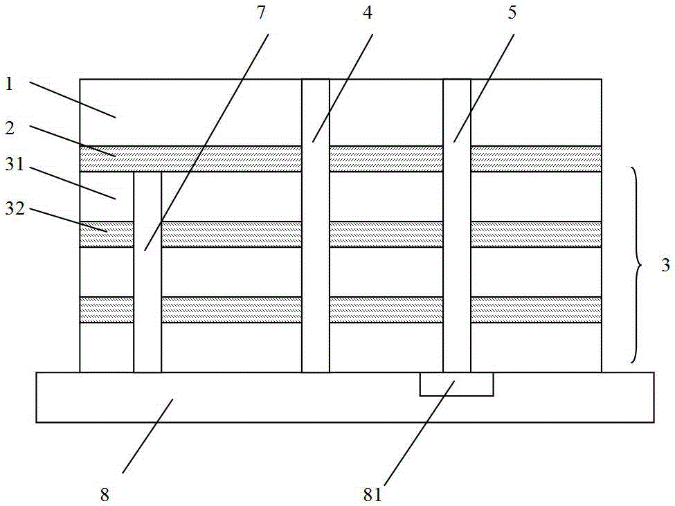
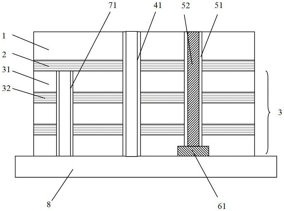
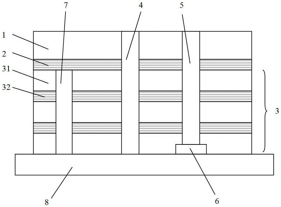
[0044] see figure 2 , a microwave digital device, including a composite circuit board and a metal casing 8 .

[0045] The composite circuit board includes a microwave signal board 1 , a microwave board prepreg 2 and a digital multilayer board 3 .

[0046] The microwave signal board 1 is connected with the digital multilayer board 3 through the microwave board prepreg 2 . The digital multilayer board 3 is connected with the metal shell 8 .

[0047] The side of the composite circuit board facing the metal shell 8 is the bottom surface, and the other side of the composite circuit board is the top surface.

[0048] The digital multilayer board 3 includes a digital signal board 31 and a digital board prepreg 32 . Adjacent digital signal boards 31 are connected together through digital board prepregs 32 . It is characterized by:

[0049] A b...


PUM


Abstract

The invention provides a microwave digital apparatus and a processing method therefor for solving the structural shortcomings of a conventional microwave digital composite substrate in performing separation of a digital signal from a grounding signal. The microwave digital apparatus comprises a composite circuit board and a metal shell; a back-drilling blind hole is formed in the bottom surface of the composite circuit board; and one side, facing to the composite circuit board, of the metal shell is a smooth plane, namely, the blind hole is not formed in one side, facing to the composite circuit board, of the metal shell. The processing method for the microwave digital apparatus comprises 13 continuous steps. The microwave digital apparatus and the processing method therefor have the beneficial effects that the processing on the metal shell is avoided; the processing method is more convenient than the former structural processing method, and a lower overall processing cost, and a higher processing efficiency are realized.

Description

technical field [0001] The invention belongs to the technical field of circuit processing, and in particular relates to a microwave digital device and a processing method thereof. Background technique [0002] At present, the method of separating the digital signal and the ground signal in the composite multilayer board is mainly realized by processing the metal shell connected to the composite multilayer board. The specific method is as follows: [0003] Traditional microwave-digital composite substrates lead digital signals and ground signals to the last layer through metallized through holes, and the holes connected to digital signals are separated from the holes connected to ground signals through isolation regions. But they are all on the same plane (they are all connected to the last layer), when the board is loaded into the metal shell 8, the last layer of the board is connected to the metal shell 8, then the last layer of the board is connected to the hole of the dig...

Claims


Application Information

Patent Timeline
IPC IPC(8): H05K1/02H05K3/46H05K5/04
CPCH05K1/0256H05K3/0094H05K3/4611H05K5/04H05K2201/0753H05K2201/09527
Inventor 管美章贾亮陈彦青崔良端王学军朱正大李晓丽朱忠翰沈岳峰
Owner ANHUI SUN CREATE ELECTRONICS
Learn More