Manufacturing method of circuit board

A manufacturing method and circuit board technology, applied in the directions of printed circuit manufacturing, printed circuit, printed circuit secondary treatment, etc., can solve the problems of easy oxidation and scratches on the surface of gold fingers, and achieve the effect of not being oxidized and scratched

Inactive Publication Date: 2016-03-16
FAIR RAYS ELECTRONICS TECH SHENZHEN LTD
View PDF5 Cites 16 Cited by
  • Summary
  • Abstract
  • Description
  • Claims
  • Application Information

AI Technical Summary

Problems solved by technology

[0004] In view of this, the present invention provides a method for manufacturing a circuit board to solv

Method used


Image

  • Manufacturing method of circuit board

Examples


Embodiment Construction

[0017] In order to make the object, technical scheme and advantages of the present invention clearer, the following combination Attached picture and embodiments, the present invention will be further described in detail. It should be understood that the specific embodiments described here are only used to explain the present invention, and are not intended to limit the present invention.

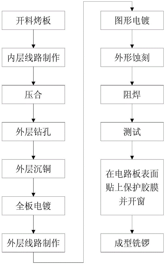
[0018] The invention provides a method for manufacturing a circuit board, comprising the following steps: cutting a baking plate; making an inner circuit; laminating; drilling the outer layer; sinking copper on the outer layer; electroplating the whole board; making the outer circuit; pattern electroplating Shape etching; Solder resistance; Testing; Forming milling; Before the forming milling step, there is also a step: sticking a protective film on the surface of the circuit board and opening a window; The milling path that the cutting tool passes through when cutting.

[0019] Since the...


PUM


Abstract

The invention belongs to the field of printed circuit board equipment, and particularly relates to a manufacturing method of a circuit board. The method comprises the following steps: carrying out cutting and board baking; fabricating an inner-layer line; carrying out lamination; drilling an outer layer; carrying out outer copper deposition; carrying out full-plate electroplating; fabricating an outer-layer line; carrying out pattern plating; carrying out appearance etching; carrying out resistance welding; carrying out a test; carrying out molding and milling; and the like, and also comprises a step of attaching a protecting adhesive film to the surface of the circuit board and windowing before the molding and milling step, wherein the windowing position of the protective adhesive film is a milling path through which an end-mill passes in the milling process. The protecting adhesive film is attached to the surface of the circuit board and is windowed, so that the target that the golden finger surface of the circuit board is not oxidized or scratched is achieved.

Description

technical field [0001] The invention belongs to the field of printed circuit board equipment, and in particular relates to a method for manufacturing a circuit board. Background technique [0002] The printed circuit board is one of the important parts of the electronics industry, the support of electronic components, and the carrier of electrical connections. With the development of multi-functionality, high precision and diversification of electronic terminals, higher requirements are placed on the quality of circuit boards. Therefore, strict quality control is required in the process of making circuit boards. [0003] The gold plating on the gold finger of the battery circuit board is generally 30 microinches, which is more expensive, and the customer has very strict requirements on the surface appearance of the gold finger. Therefore, care must be taken in the molding process after surface treatment + gold plating on the gold finger of the contact Be careful, and now mo...

Claims


Application Information

Patent Timeline
IPC IPC(8): H05K3/28
CPCH05K3/282H05K2203/1383H05K2203/304
Inventor 张优胜彭江义
Owner FAIR RAYS ELECTRONICS TECH SHENZHEN LTD
Why Eureka
Try Eureka