Display substrate, manufacturing method thereof, and display device
A technology for a display substrate and a manufacturing method, which can be applied to instruments, nonlinear optics, optics, etc., can solve the problems of lowering the contrast of display devices, and achieve the effects of reducing reflectivity, improving quality, and reducing influence.
- Summary
- Abstract
- Description
- Claims
- Application Information
AI Technical Summary
Problems solved by technology
Method used
Image

Examples
Embodiment 1
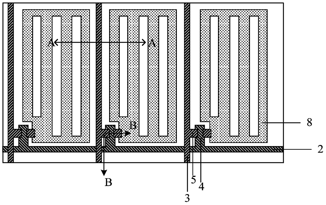
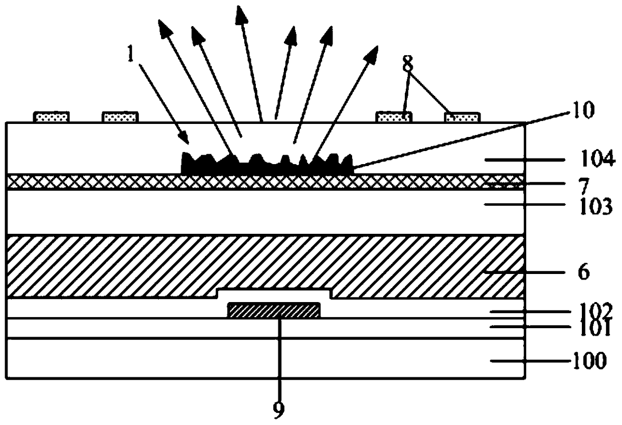
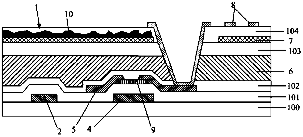
[0026] figure 1 A schematic diagram showing the structure of the display substrate in this embodiment, figure 2 express figure 1 Section along A-A Figure 1 , image 3 express figure 1 Section along B-B Figure 1 , Figure 4 express figure 1 Section along A-A Figure II , Figure 5 express figure 1 Section along B-B Figure II .
[0027] combine Figure 1-Figure 5 As shown, a display substrate is provided in this embodiment, and the display substrate includes a black matrix 1, and the surface of the black matrix 1 close to the display side is uneven, so as to reduce the light reflected by the black matrix 1 to the display side and reduce the brightness of the display panel. Reflectivity reduces the impact on the contrast of the display screen and improves the quality of the display screen.
[0028] The display substrate may be a color filter substrate or a COA array substrate.
[0029] The technical solution of the present invention is especially suitable for th...
Embodiment 2
[0046] This embodiment provides a display device, including the display substrate in Embodiment 1. Since the reflectivity of the black matrix is reduced, the specular reflection effect of the black matrix is reduced, and the quality of the display image is improved.
[0047] The display device may specifically be any product or component with a display function such as a display panel, electronic paper, a mobile phone, a tablet computer, a television, a monitor, a notebook computer, a digital photo frame, a navigator, and the like.
Embodiment 3
[0049] Based on the same inventive idea as the technical solution in Embodiment 1, this embodiment provides a method for manufacturing a display substrate, the method includes a step of forming a black matrix, and the step of forming a black matrix includes:
[0050] An uneven structure is formed on the surface of the black matrix near the display side.
[0051] The black matrix prepared by the above manufacturing method has an uneven surface, which effectively reduces the light reflected to the display side, ensures the contrast of the display substrate, and improves the quality of the display screen.
[0052] Wherein, the step of forming the black matrix includes the step of forming a first sublayer, the surface of the first sublayer is uneven, and is used to provide the black matrix with an uneven surface.
[0053] The first sub-layer can be made of metallic material or insulating material.
[0054] Further, the step of forming the black matrix also includes:
[0055] For...
PUM
 Abstract
Description
Claims
Application Information
 - R&D
- Intellectual Property
- Life Sciences
- Materials
- Tech Scout
- Unparalleled Data Quality
- Higher Quality Content
- 60% Fewer Hallucinations
Browse by: Latest US Patents, China's latest patents, Technical Efficacy Thesaurus, Application Domain, Technology Topic, Popular Technical Reports.
© 2025 PatSnap. All rights reserved.Legal|Privacy policy|Modern Slavery Act Transparency Statement|Sitemap|About US| Contact US: help@patsnap.com