semiconductor storage device

A storage device and semiconductor technology, applied in information storage, static memory, read-only memory, etc., can solve problems such as uneven shape, uneven ion implantation, and bit errors

Active Publication Date: 2019-08-23
WINBOND ELECTRONICS CORP
View PDF7 Cites 0 Cited by
  • Summary
  • Abstract
  • Description
  • Claims
  • Application Information

AI Technical Summary

Problems solved by technology

It is worth noting that the cell near the group selection transistor is uneven due to photolithography, and the bit error tends to increase due to the uneven ion implantation when forming the diffusion layer.

Method used


Image

  • semiconductor storage device
  • semiconductor storage device
  • semiconductor storage device

Examples


Embodiment Construction

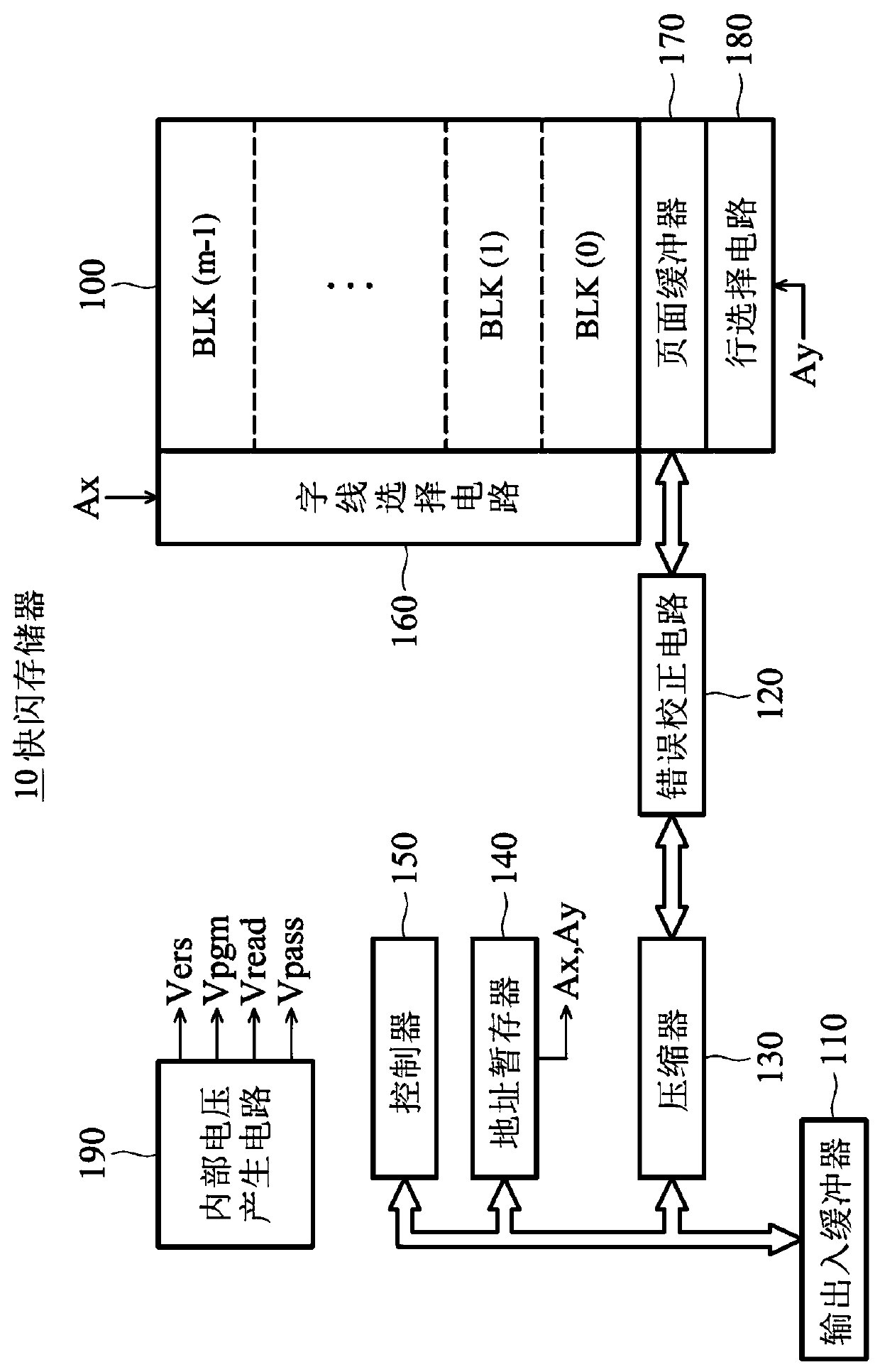
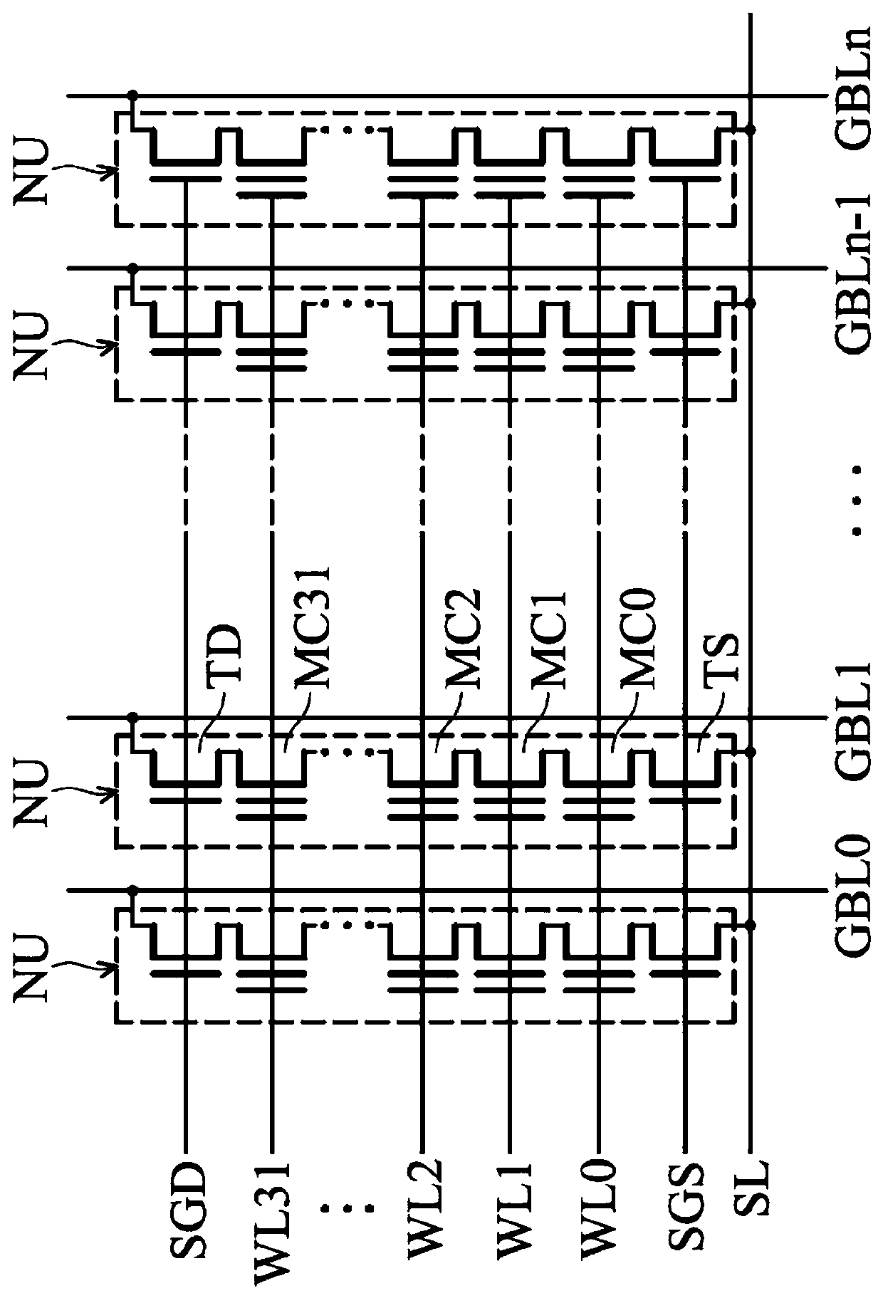
[0049] Embodiments of the present invention will be described in detail below with reference to the drawings. The present invention can be applied to nonvolatile memories with various types of memory structures, so an ideal type of NAND flash memory is taken as an example for illustration. In addition, each part is emphasized in illustration for easy understanding, and attention should be paid to the difference in scale of an actual device.

[0050] figure 1Shown is a schematic diagram of a typical flash memory pertaining to embodiments of the present invention. However, the flash memory shown here is only used as an example, and is not intended to limit the concept of the present invention. The flash memory 10 shown in this embodiment includes a memory array 100 in which a plurality of memory cells are arranged in rows and columns, an I / O buffer 110 that is connected to external I / O terminals and maintains I / O data, and reads out bit data and The error correction circuit 1...


PUM


Abstract

The invention provides a semiconductor storage apparatus. The apparatus comprises a storer array, a data maintaining assembly for maintaining data read from the storer array or maintaining data written into the storer array, an external output and input endpoint, a coupling data maintaining assembly, an error correction assembly for detecting or correcting the error of the data input to the data maintaining assembly or the output data from the data maintaining assembly, and a compression assembly coupled between the external output and input endpoint and the error correction assembly and used for compressing or extending the data, wherein the compression assembly compresses data provided by the external output and inlet endpoint, provides the compressed data to the error correction assembly, extends the data provided by the error correction assembly and provides the extended data to the external output and input endpoint. The compression assembly is configured to compress or extend the data in order to shorten the output and input time of the data.

Description

technical field [0001] The present invention relates to a semiconductor memory device, in particular to compression extension or error correction of input and output data. Background technique [0002] Semiconductor memories such as flash memory and dynamic random access memory increase year by year with circuit density, making it difficult to manufacture defective or defective products. Therefore, in the case of memory chips, lengthy schemes are required to discover and compensate for physical defects of memory elements that occur during the manufacturing process. For example, verbose planning is used to compensate for physically defective memory elements in large-scale memory arrangements. In addition, in addition to the physical compensation based on the large memory, the semiconductor memory also includes an error correction circuit (ECC, Error Checking Correction) corresponding to software errors. [0003] In the case of NAND flash memory, due to repeated programming ...

Claims


Application Information

Patent Timeline
Patent Type & Authority Patents(China)
IPC IPC(8): G11C16/06G11C29/44
Inventor 村上洋树
Owner WINBOND ELECTRONICS CORP
Why Eureka
Try Eureka