A kind of semiconductor device and its manufacturing method and electronic device

A manufacturing method and semiconductor technology, applied in the direction of semiconductor device, semiconductor/solid-state device manufacturing, circuits, etc., can solve the problems of difficult process, inability to operate wafers, and high cost, and achieve lower production costs, good ohmic contact, and ensure safety. The effect of transmission

Active Publication Date: 2019-04-09
SEMICON MFG INT (SHANGHAI) CORP
View PDF4 Cites 0 Cited by
  • Summary
  • Abstract
  • Description
  • Claims
  • Application Information

AI Technical Summary

Problems solved by technology

However, the cost of this method is relatively high, which will increase the production cost
[0004] Another method is the method of temporary bonding / de-bonding; but this method is very difficult when making a double-sided process on a thinned silicon wafer, especially in the alloy of the back metal. During the chemical process, the temperature is too high, which may lead to the failure of the temporary bonding (glue) on the front side, resulting in the inability to operate the wafer

Method used


Image

  • A kind of semiconductor device and its manufacturing method and electronic device
  • A kind of semiconductor device and its manufacturing method and electronic device
  • A kind of semiconductor device and its manufacturing method and electronic device

Examples


Embodiment 1

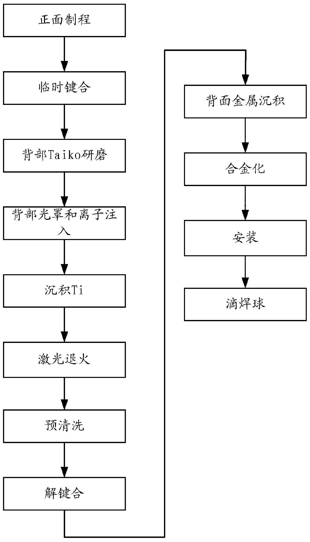
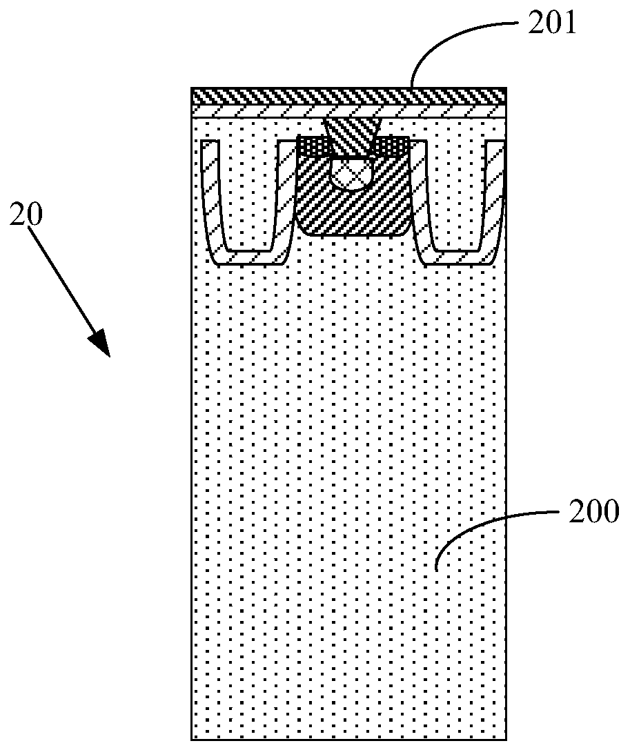
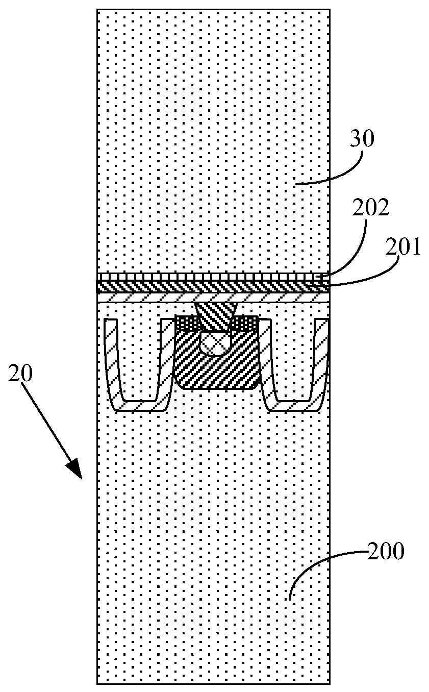
[0066] Below, refer to Figure 2A-Figure 2H and image 3 The method of the embodiment of the present invention is described in detail.

[0067] in Figure 2A-Figure 2H A schematic cross-sectional view of a device obtained by sequentially implementing the method of the embodiment of the present invention is shown; image 3 A process flow diagram of sequential implementation of the method of the embodiment of the present invention is shown.

[0068] First, if Figure 2A As shown, a device wafer 20 is provided, the device wafer includes a substrate 200, and the substrate 200 may be at least one of the materials mentioned below: silicon, silicon-on-insulator (SOI), stack-on-insulator Silicon (SSOI), silicon germanium on insulator (S-SiGeOI) and silicon germanium on insulator (SiGeOI), etc. Further, the substrate may also be an N-type substrate or a P-type substrate. It can also be an N-type lightly doped substrate.

[0069] An isolation structure is formed in the substrate,...

Embodiment 2

[0089] refer to Figure 4 The IGBT device of the embodiment of the present invention will be further described.

[0090] An embodiment of the present invention provides an insulated gate bipolar transistor manufactured by the method in Embodiment 1, including:

[0091]The substrate 400 and the front structure formed on the front surface of the substrate 400 . The substrate 400 may be at least one of the materials mentioned below: silicon, silicon-on-insulator (SOI), silicon-on-insulator (SSOI), silicon-germanium-on-insulator (S-SiGeOI) and silicon-on-insulator Silicon germanium (SiGeOI), etc. Further, the substrate 400 may also be an N-type substrate or a P-type substrate, or an N-type lightly doped substrate.

[0092] An isolation structure is formed in the substrate, and the isolation structure is a shallow trench isolation (STI) structure or a local oxide of silicon (LOCOS) isolation structure. Various well structures and channel layers on the surface of the substrate a...

Embodiment 3

[0099] The present invention also provides an electronic device including the above-mentioned semiconductor device.

[0100] The electronic device also has the above advantages due to the excellent performance and reliability of the included semiconductor device.

[0101] The electronic device can be any electronic product or equipment such as mobile phone, tablet computer, notebook computer, netbook, game console, TV, VCD, DVD, navigator, camera, video recorder, voice recorder, MP3, MP4, PSP, etc. It is an intermediate product with the above-mentioned semiconductor device, for example: a mobile phone motherboard with the integrated circuit, etc.


PUM


Abstract

The invention provides a semiconductor device, a manufacturing method thereof and an electronic apparatus. The manufacturing method comprises the steps of providing a device wafer which includes a substrate and a front structure formed at the front of the substrate; providing a support wafer, and bonding the support wafer and the front of the device wafer temporarily through an adhesive layer; thinning the back of the device wafer; forming a collector region on the back of the device wafer; forming, on the surface of the collector region, a collector electrode which is an alloy having a film forming temperature lower than 200 DEG C; and de-bonding to separate the device wafer from the support wafer. The preparation method of the invention can achieve good ohmic contact between the collector electrode and the collector region by adopting the collector electrode having a film forming temperature lower than 200 DEG C and without the need of alloying treatment. The use of a costly Taiko wafer can be avoided, the production cost is reduced, secure transmission of the device wafer is ensured without the occurrence of fragmentation problem, and the yield is therefore improved.

Description

technical field [0001] The invention relates to the technical field of semiconductors, in particular to a semiconductor device, a manufacturing method thereof, and an electronic device. Background technique [0002] In semiconductor technology, an insulated gate bipolar transistor (Insulated Gate Bipolar Transistor, referred to as IGBT) is a composite fully-controlled voltage-driven power semiconductor composed of a bipolar transistor (BJT) and an insulated gate field effect transistor (MOSFET). The device has both the advantages of high input impedance of MOSFET and low conduction voltage drop of power transistor (ie, giant transistor, referred to as GTR). Therefore, IGBT, as a necessary switching device, is widely used in inverters and inverters. Converter and other circuit structures. [0003] In order to reduce energy loss and improve heat dissipation, it is often necessary to thin the IGBT device. However, the thinner the wafer, the more likely it will be cracked and d...

Claims


Application Information

Patent Timeline
Patent Type & Authority Patents(China)
IPC IPC(8): H01L29/739H01L29/08H01L21/331
Inventor 陈福成向阳辉
Owner SEMICON MFG INT (SHANGHAI) CORP
Why Eureka
Try Eureka