Infrared sensor and packaging structure thereof and preparation method thereof

A technology of infrared sensor and packaging structure, which is applied in semiconductor devices, electric radiation detectors, final product manufacturing, etc., can solve the problems of high cost, high cost, low production capacity, etc., reduce process cost and difficulty, and increase effective fill factor , the effect of reducing the preparation cost

Active Publication Date: 2016-03-30
SHANGHAI JUGE ELECTRONICS TECH
View PDF3 Cites 15 Cited by
  • Summary
  • Abstract
  • Description
  • Claims
  • Application Information

AI Technical Summary

Problems solved by technology

At present, the commonly used packaging technologies are device-level packaging and multi-chip batch packaging technologies. However, these packaging technologies have low infrared transmittance, complex processes, high costs, and

Method used


Image

  • Infrared sensor and packaging structure thereof and preparation method thereof
  • Infrared sensor and packaging structure thereof and preparation method thereof
  • Infrared sensor and packaging structure thereof and preparation method thereof

Examples


Example Embodiment

[0027] The present invention will be described in further detail below in conjunction with the accompanying drawings.

[0028] The present invention provides an infrared sensor and its packaging structure, wherein the infrared sensor and its packaging structure include:

[0029] The readout circuit substrate is used to collect and process the output signal of the infrared sensor;

[0030] The infrared sensor unit, including some pixels in the infrared sensor array, is used to convert the infrared radiation incident on the infrared sensor unit into an electrical signal and output it from the readout circuit substrate;

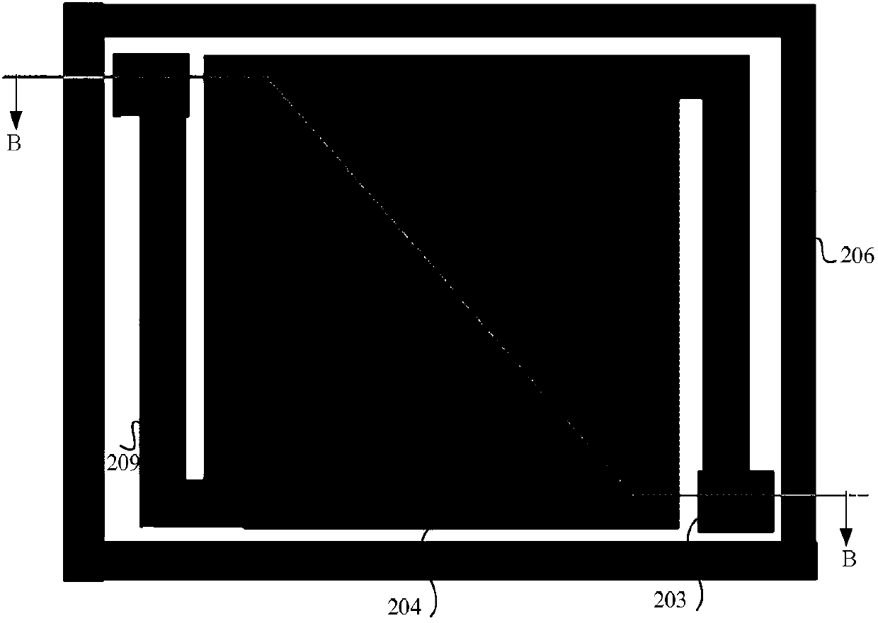
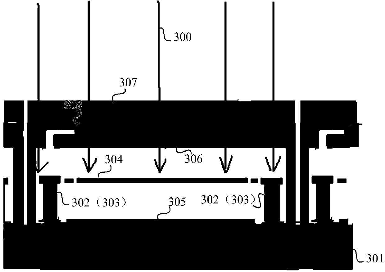
[0031] The vacuum microcavity structure encapsulates the infrared sensor unit in the vacuum environment of its inner area, and the vacuum microcavity structure includes a support shell with a release channel, an infrared anti-reflection device located above the support shell and blocking the release channel Membrane, a getter thin film inside the vacuum microca...


PUM


Abstract

The invention provides an infrared sensor and packaging structure thereof and a preparation method thereof. The infrared sensor and packaging structure thereof comprises a reading circuit substrate for collecting and processing output signals of infrared sensors; an infrared sensor unit comprising a part of pixels in an infrared sensor array and used for converting infrared radiation incident to the infrared sensor unit into electrical signals, which are output by the reading circuit substrate; and a vacuum micro-cavity structure for packaging the infrared sensor unit in the vacuum environment of an inner region thereof. The vacuum micro-cavity structure comprises a support housing having a release channel, an infrared antireflection film arranged on the upper surface of the support housing and for blocking the release channel, and a getter film arranged inside the vacuum micro-cavity structure. According to the scheme, pixel-level packaging of the infrared sensors can be realized, absorption efficiency of the infrared sensors for the infrared radiation can be increased, and sensitivity of the infrared sensors is improved.

Description

technical field [0001] The invention relates to the technical field of semiconductors, in particular to an infrared sensor and its packaging structure, and a method for preparing the infrared sensor and its packaging structure. Background technique [0002] In the prior art, when the infrared sensor is packaged, a bonding process is used to seal the entire infrared sensor array in a package composed of a ceramic or metal shell and an infrared window in a vacuum environment, such as figure 1 shown in . At present, the commonly used packaging technologies are device-level packaging and multi-chip batch packaging technologies. However, these packaging technologies have low infrared transmittance, complex processes, high costs, and low production capacity. Moreover, the bonding process requires special equipment and process, which is difficult and costly, and is incompatible with standard integrated circuit processing and integrated circuit packaging processes. Contents of th...

Claims


Application Information

Patent Timeline
IPC IPC(8): H01L31/0203H01L31/0232H01L31/18G01J5/10
CPCY02P70/50
Inventor 陈学枝沈憧棐黄新龙
Owner SHANGHAI JUGE ELECTRONICS TECH
Why Eureka
Try Eureka