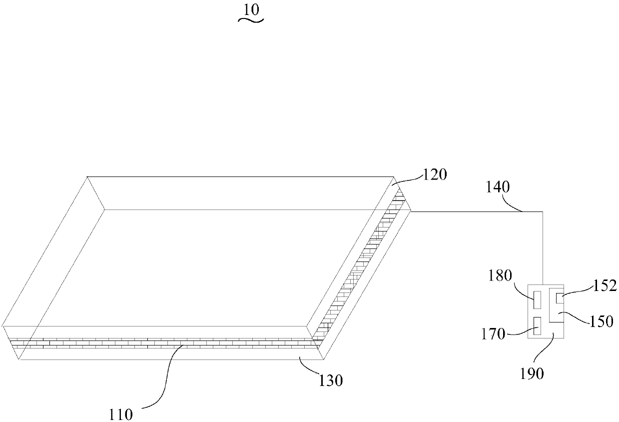
Heating pad
A heating pad and heating film technology, applied in ohmic resistance heating, electric heating devices, instruments, etc., can solve problems such as poor safety performance, high power supply voltage, and inability to heat mouse pads
- Summary
- Abstract
- Description
- Claims
- Application Information
AI Technical Summary
Problems solved by technology
Method used
Image
Examples
preparation example Construction
[0108] The preparation method of the above-mentioned heating film 210 is relatively simple, saving time and material cost. At the same time, the electrode layer is prepared by using metal foil, which has good conductivity and is beneficial to control the uniformity of the temperature of the heating film.
[0109] Preferably, the thickness of the first adhesive layer 213 and the second adhesive layer 217 is 25-75 μm.
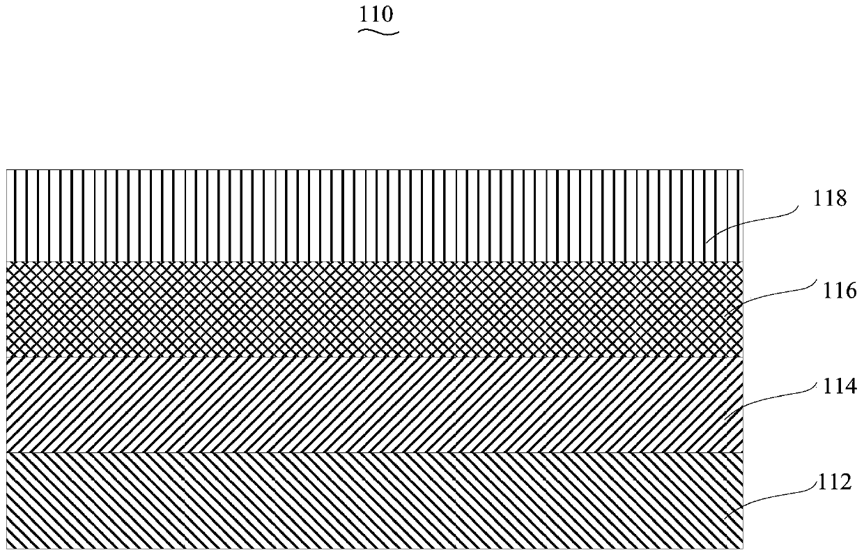
[0110] see Figure 5 , the structure of the heating pad in another embodiment is substantially the same as that of the heating pad 10, the difference is that in the illustrated embodiment, the heating film 410 of the heating pad includes a first insulating layer 412, a conductive layer 414, and an electrode stacked in sequence. layer 416 , a second adhesive layer 417 and a second insulating layer 418 . The second insulating layer 418 is bonded to the electrode layer 416 through the second insulating layer 418 . Preferably, the material of the second adhesive la...
Embodiment 1
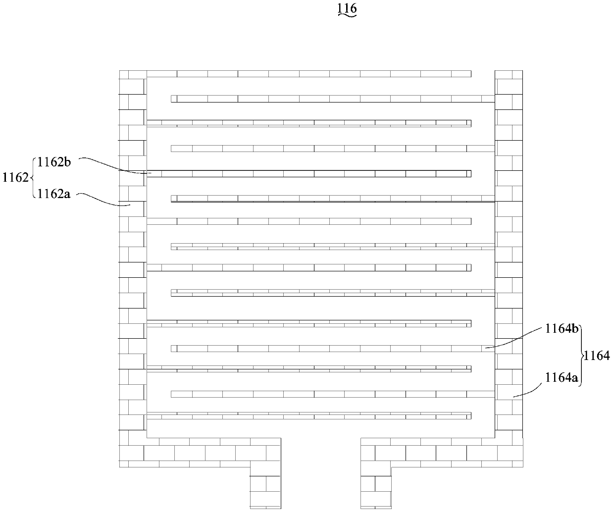
[0127] Please also see image 3 and Figure 4 , single-layer graphene is used as the conductive layer of the heating film, and the electrode layer is printed with silver paste.
[0128] 1. Transfer a layer of graphene on the PET (first insulating layer) with an area of 150mm×150mm and a thickness of 125μm. The graphene has been doped and the square resistance is 250Ω / □;
[0129] 2. Use screen printing equipment to print the silver paste electrode pattern on the transferred graphene, the shape of the pattern is as follows: image 3 As shown, the distance between the positive inner electrode and the negative inner electrode is 6mm, the length of the positive inner electrode and the negative inner electrode is 108mm, and the width is 1mm, a total of 15, the width of the positive bus bar and the negative bus bar is 8mm, and the thickness of the silver paste is 25μm;
[0130] 3. Bake the printed electrode layer in an oven to solidify the silver paste. The baking temperature is ...
Embodiment 2
[0141] In this embodiment, two layers of graphene are used as the conductive layer of the heating film, and the electrode layer is printed with silver paste.
[0142] 1. Transfer two layers of graphene as the conductive layer on the PET (first insulating layer) with an area of 120mm×120mm and a thickness of 125μm. The graphene has been doped and the square resistance is 120Ω / □;
[0143] 2. Use screen printing equipment to print the silver paste electrode layer on the transferred conductive layer, and the pattern shape is as follows: Figure 9 As shown, the outer diameter of the bus bar is 96mm, the inner electrode spacing is 6mm, the width is 1mm, the width of the bus bar is 8mm, and the thickness of the silver paste is 25μm;
[0144] 3. Bake the printed electrode pattern in an oven to solidify the silver paste. The baking temperature is 130°C for 40 minutes.
[0145] In this case, connect the lead wires to the positive and negative poles of the 5V power supply respectively...
PUM
 Abstract
Description
Claims
Application Information


