High-density three-dimensional stacking and assembling method for electronic modules

A three-dimensional stacking, electronic module technology, applied in the computer field, to improve the integration density and solve the effect of heat dissipation

Active Publication Date: 2016-03-30
XIAN AVIATION COMPUTING TECH RES INST OF AVIATION IND CORP OF CHINA
View PDF4 Cites 3 Cited by
  • Summary
  • Abstract
  • Description
  • Claims
  • Application Information

AI Technical Summary

Problems solved by technology

[0009] Aiming at the need for high-density assembly of high-performance computers in harsh environments, the present invention proposes a high-density three-dimensional stacking assembly method, which im

Method used


Image

  • High-density three-dimensional stacking and assembling method for electronic modules
  • High-density three-dimensional stacking and assembling method for electronic modules
  • High-density three-dimensional stacking and assembling method for electronic modules

Examples


Embodiment Construction

[0032] The present invention will be described in detail below in conjunction with the accompanying drawings.

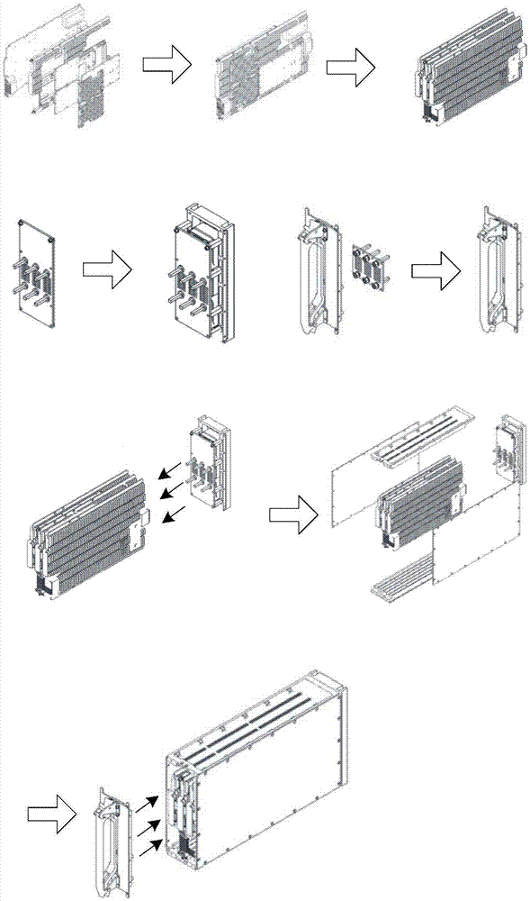
[0033] A high-density three-dimensional stacking and assembling method for electronic modules, which consists of multiple functional circuit boards, functional circuit sub-cards, front motherboards, rear motherboards and other circuit components, as well as the rear cover of the chassis, the front cover of the chassis, the left cover of the chassis, The structural components such as the right cover plate of the chassis, the upper frame of the chassis, and the lower frame of the chassis are stacked through multi-dimensional and multi-level methods, such as figure 1 shown.

[0034] The specific stacking and assembly steps are as follows: figure 2 Shown:

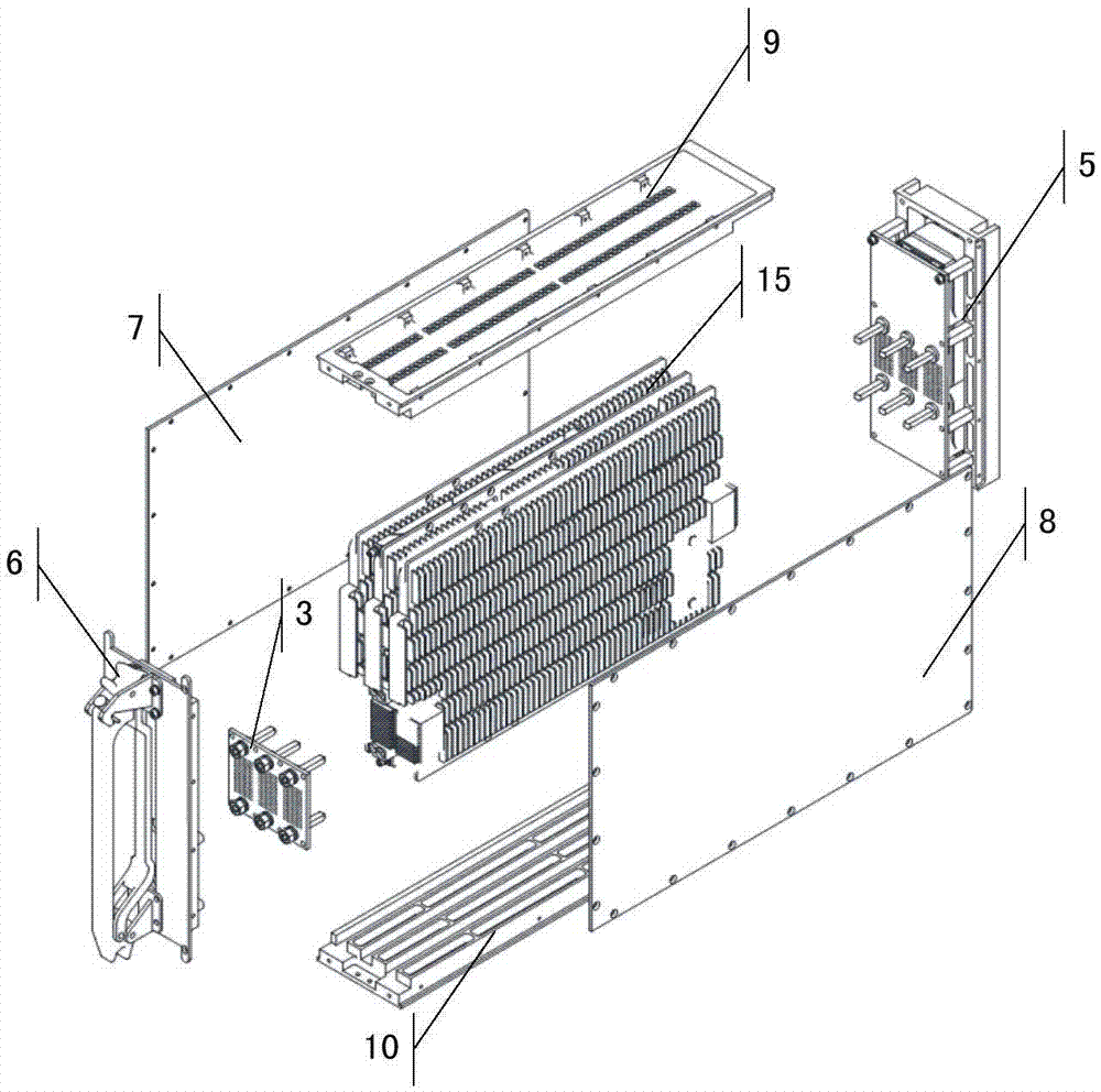
[0035] 1] Through the inter-board parallel connector, perform parallel stacking of functional circuit boards, functional circuit sub-cards and heat dissipation plates to complete functional circuit components, such...


PUM


Abstract

The invention provides a high-density three-dimensional stacking and assembling method for electronic modules. The stacking and assembling method comprises the following steps: completing parallel stacking for functional circuit boards, function circuit sub cards and a radiating plate, and forming a functional circuit module; completing assembling for a back mother board and a machine case back cover board, and assembling for a front mother board and a machine case front cover board; enabling multiple functional circuit modules to be placed horizontally, and perpendicularly stacking the functional circuit modules with a back mother board cover board module through a bottom board connector; coating a machine case left cover board, a machine case right cover board, a machine case upper frame and a machine case lower frame for forming a machine case body; enabling a three-dimensional stacked body to be fixed in the machine case upper frame and the machine case lower frame through locking strips that are positioned on the functional circuit boards; completing the assembling and stacking for the front mother board cover board module; and finally forming the high-density electronic module with an anti-severe environment function. Compared with the existing electronic module assembling method in severe environments, the high-density three-dimensional stacking and assembling method provided by the invention has the advantages of high assembling density, light structural weight, high radiating efficiency, high support for high-speed signals, strong shock-proof and anti-impact capability, and the like.

Description

technical field [0001] The invention belongs to the field of computers and provides a method for high-density three-dimensional stacking and assembling of electronic modules. Background technique [0002] The assembly of high-density electronic modules has always been one of the difficulties in computer design in harsh environments. On the one hand, it is required that the electronic module can increase the integration density and reduce the volume and weight as much as possible; on the other hand, it is required that the computer can work normally in harsh environments such as high temperature, strong vibration, and strong impact. [0003] Traditional high-density electronic module assembly adopts the "chassis-board" assembly method. First, complete the machine installation of each component of the chassis and the machine installation of the board and heat sink, then fix the motherboard in the chassis, complete the assembly of the panel connector, and finally insert the bo...

Claims


Application Information

Patent Timeline
IPC IPC(8): H05K7/14
CPCH05K7/1422
Inventor 王乐蔡晓乐郭建平白振岳杨明明段宇博
Owner XIAN AVIATION COMPUTING TECH RES INST OF AVIATION IND CORP OF CHINA
Why Eureka
Try Eureka