Manufacturing method of surface plasma lens
A technology of surface plasma and manufacturing method, applied in the field of ion lens manufacturing, can solve the problems of large volume and complex structure, and achieve the effects of small volume, simple manufacturing method and improved efficiency
- Summary
- Abstract
- Description
- Claims
- Application Information
AI Technical Summary
Problems solved by technology
Method used
Image

Examples
Embodiment Construction
[0028] In order to make the above objects, features and advantages of the present invention more comprehensible, specific implementations of the present invention will be described in detail below in conjunction with the accompanying drawings.
[0029] In the following description, numerous specific details are set forth in order to provide a thorough understanding of the present invention. However, the present invention can be implemented in many other ways different from those described here, and those skilled in the art can make similar extensions without violating the connotation of the present invention, so the present invention is not limited by the specific implementations disclosed below.
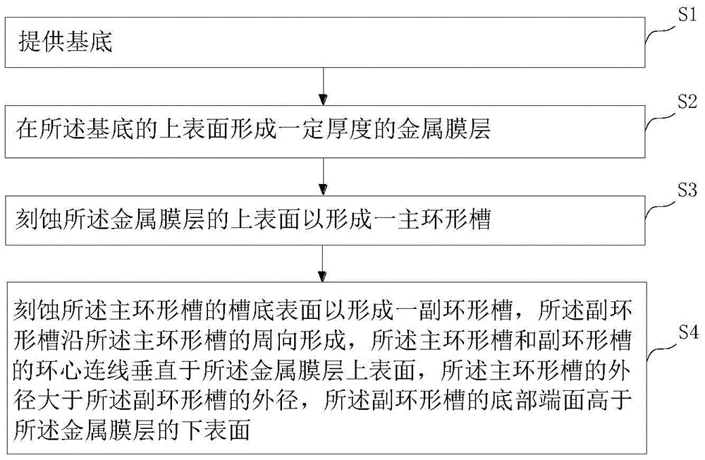
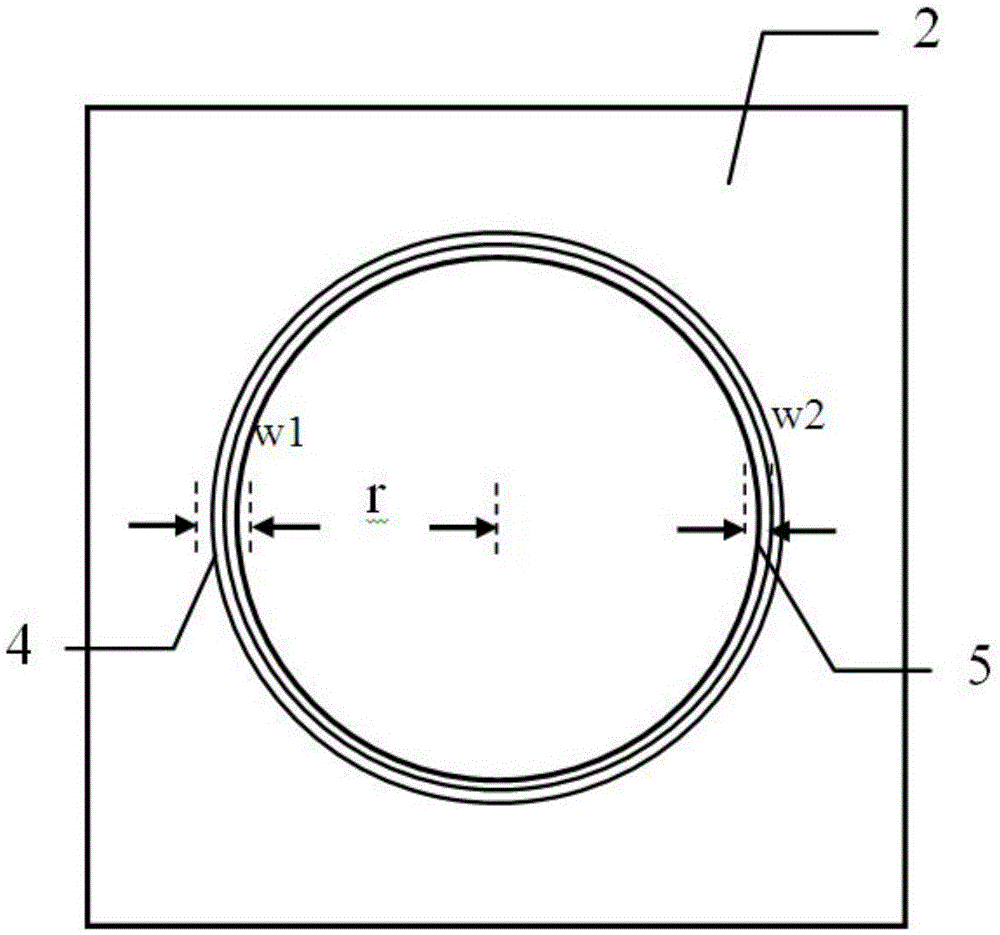
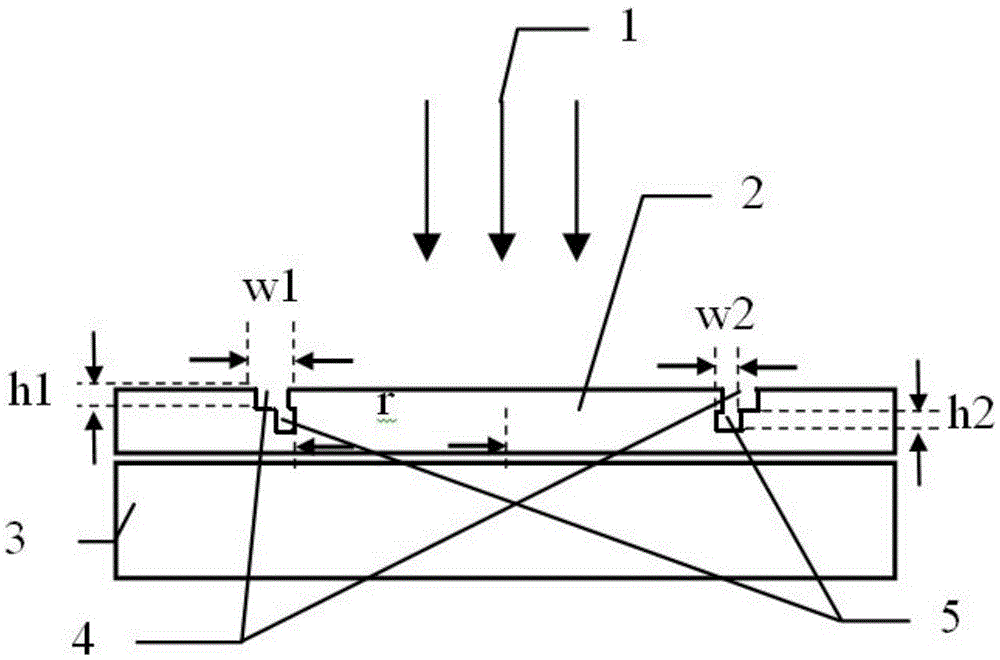
[0030] see figure 1 , the surface plasmon lens manufacturing method of the embodiment of the present invention, comprises the following steps:
[0031] S1: Provide the base;
[0032] S2: forming a metal film layer with a certain thickness on the upper surface of the substrate;
...
PUM
| Property | Measurement | Unit |
|---|---|---|
| The inside diameter of | aaaaa | aaaaa |
| Thickness | aaaaa | aaaaa |
Abstract
Description
Claims
Application Information
 - R&D
- Intellectual Property
- Life Sciences
- Materials
- Tech Scout
- Unparalleled Data Quality
- Higher Quality Content
- 60% Fewer Hallucinations
Browse by: Latest US Patents, China's latest patents, Technical Efficacy Thesaurus, Application Domain, Technology Topic, Popular Technical Reports.
© 2025 PatSnap. All rights reserved.Legal|Privacy policy|Modern Slavery Act Transparency Statement|Sitemap|About US| Contact US: help@patsnap.com