Liquid crystal display panel and driving method thereof

A liquid crystal display panel and substrate technology, applied in static indicators, instruments, nonlinear optics, etc., can solve the problems of high process and circuit complexity, high cost, and reduce the output voltage range of data-driven ICs, etc., to achieve the best picture display effect, the effect of reducing output voltage and reducing power consumption

Inactive Publication Date: 2016-04-06
KUSN INFOVISION OPTOELECTRONICS
View PDF11 Cites 16 Cited by
  • Summary
  • Abstract
  • Description
  • Claims
  • Application Information

AI Technical Summary

Problems solved by technology

[0010] For data-driven ICs, the larger the output voltage range, the higher the complexity of the process and circuit, and the higher the cost
At present, the data driver IC produced by the general semiconductor process can only provide a voltage of less than 10V. If the output voltage range of the data driver IC can be reduced to less than 10V, it will be very beneficial for the selection of the source of the data driver IC and the reduction of power consumption.
As above, if you choose figure 2 The common electrode AC drive (ACV_com) shown can reduce the output voltage range of the data driver IC, but figure 2 The common electrode AC drive (ACV_com) shown is only applicable to frame inversion and row inversion, but not to column inversion and dot inversion, and cannot achieve a better picture display effect

Method used


Image

  • Liquid crystal display panel and driving method thereof
  • Liquid crystal display panel and driving method thereof
  • Liquid crystal display panel and driving method thereof

Examples


Embodiment Construction

[0039] In order to further explain the technical methods and effects of the present invention to achieve the intended purpose of the invention, the specific implementation, structure, features and effects of the present invention will be described in detail below with reference to the accompanying drawings and embodiments.

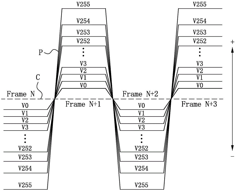
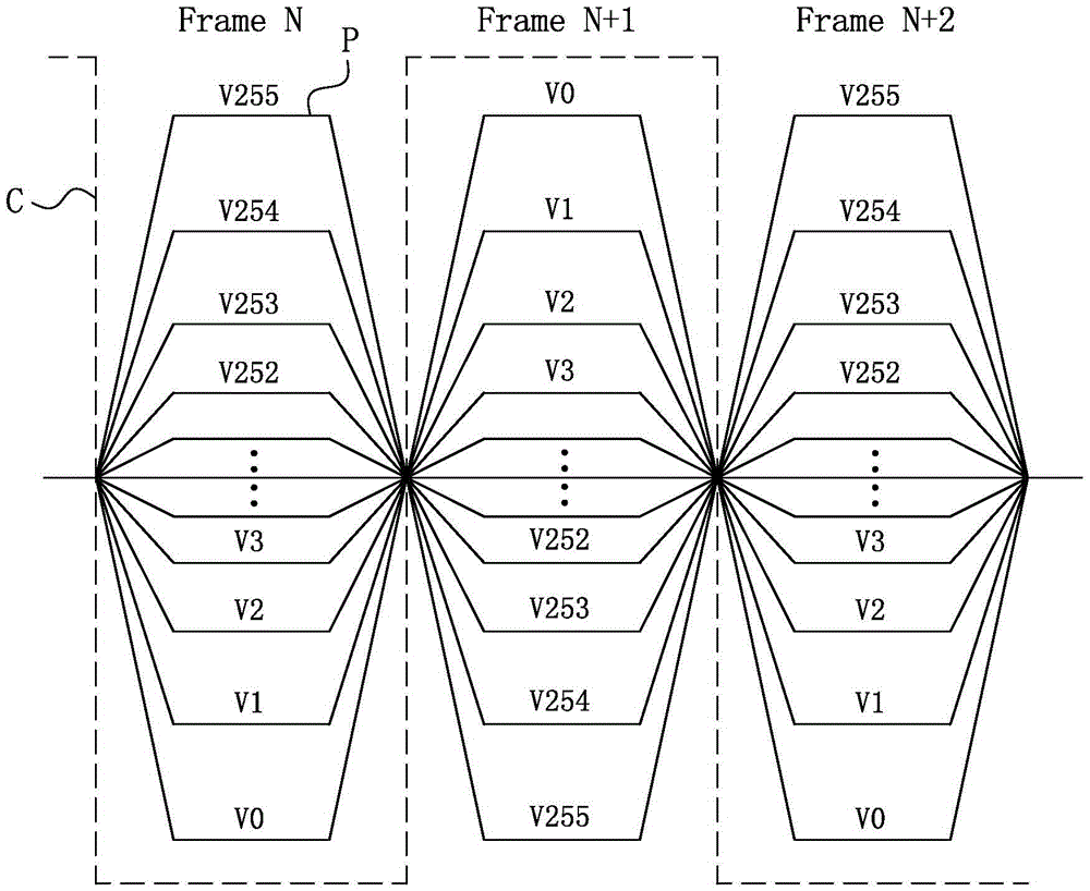
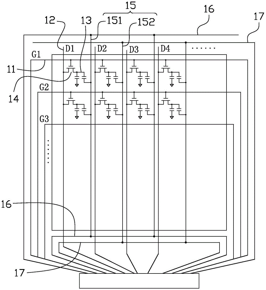
[0040] Please refer image 3 with Figure 4 The liquid crystal display panel provided by the embodiments of the present invention includes a thin film transistor array substrate, a color filter substrate (not shown), and a liquid crystal layer (not shown) sandwiched between the two. Wherein, a scan line 11 and a data line 12 are formed on the thin film transistor array substrate, wherein a plurality of scan lines 11 and a plurality of data lines 12 intersect each other to define a plurality of pixel regions, and each pixel region can be used as a sub-pixel of the display panel ( sub-pixel), a pixel electrode 13 is provided in each pixel area. Thin film transi...


PUM


Abstract

The invention provides a liquid crystal display panel and a driving method thereof. The liquid crystal display panel comprises scanning lines, data lines, pixel electrodes and common electrodes, wherein multiple scanning lines and multiple data lines are mutually intersected to define multiple pixel regions, the pixel electrodes are arranged in the pixel regions, the common electrodes are matched with the pixel regions to produce an electric field driving liquid crystal molecules to deflect, the common electrodes are divided into multiple columns mutually spaced in the directions of the data lines and include the common electrodes located in odd-number columns and the common electrodes located in even-number columns, the common electrodes located in odd-number columns are jointly connected to a first common electrode bus, and the common electrodes located in even-number columns are jointly connected to a second common electrode bus. The liquid crystal display panel inputs alternating current driving signals (AC V_com) identical in frequency but opposite in polarity respectively through the common electrodes located in odd-number columns, can achieve polarity reversal modes of column reversal and point reversal while reducing output voltage of a data drive IC and accordingly achieves a better image display effect.

Description

Technical field [0001] The present invention relates to the technical field of liquid crystal display, in particular to a liquid crystal display panel and a driving method thereof. Background technique [0002] Liquid crystal display (LCD) has the advantages of good image quality, small size, light weight, low driving voltage, low power consumption, no radiation, and relatively low manufacturing cost, and it is dominant in the flat panel display field. The liquid crystal display panel includes a color filter substrate (CF) and a thin film transistor array substrate (TFTarray) opposed to each other, and a liquid crystal layer (LClayer) sandwiched between the two. [0003] Due to the characteristics of liquid crystal, long-term application of DC voltage in one direction to it will polarize the liquid crystal. Normally driven liquid crystal must be applied with an AC electric field. The voltage applied to the pixel electrode is reversed alternately with respect to the common electrode...

Claims


Application Information

Patent Timeline
Patent Type & Authority Applications(China)
IPC IPC(8): G02F1/133G02F1/1362G09G3/36
CPCG02F1/13306G02F1/136286G09G3/3655
Inventor 房耸
Owner KUSN INFOVISION OPTOELECTRONICS
Why Eureka
Try Eureka