Method for measuring epitaxial layer in epitaxy device and epitaxy process

A measurement method and epitaxial layer technology, applied in the semiconductor field, can solve the problems of inability to use silicon epitaxy measurement, inability to directly obtain thickness values, inability to measure epitaxial layer thickness, etc., to achieve controllable epitaxy process, avoid waste, improve utilization and Effect

Active Publication Date: 2018-08-24
BEIJING NAURA MICROELECTRONICS EQUIP CO LTD
View PDF3 Cites 0 Cited by
  • Summary
  • Abstract
  • Description
  • Claims
  • Application Information

AI Technical Summary

Problems solved by technology

[0008] 1. Fourier transform infrared spectroscopy can only be used to measure the finished product after epitaxy, and cannot measure parameters such as the thickness of the epitaxial layer during the growth process
[0009] 2. Since silicon materials can absorb energy in the entire visible spectrum range, interference in the visible range cannot be used for the measurement of silicon epitaxy
In addition, this method of using visible light interference obtains an interference spectrum that varies with thickness. The accurate thickness value needs to be calculated according to time, and the thickness value cannot be directly obtained.

Method used


Image

  • Method for measuring epitaxial layer in epitaxy device and epitaxy process
  • Method for measuring epitaxial layer in epitaxy device and epitaxy process
  • Method for measuring epitaxial layer in epitaxy device and epitaxy process

Examples


Embodiment Construction

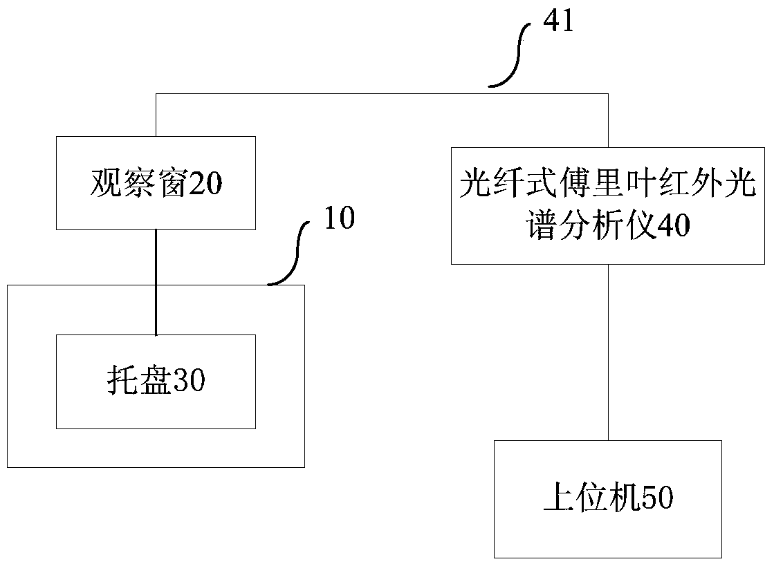
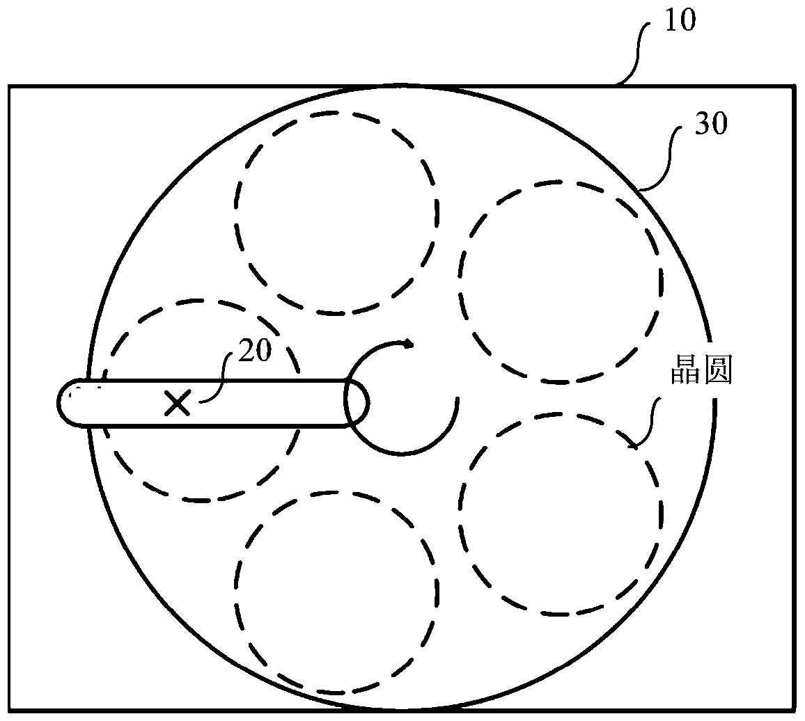
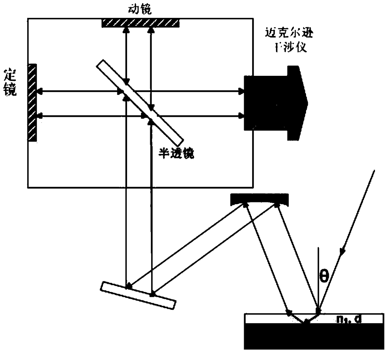
[0027] Embodiments of the present invention are described in detail below, examples of which are shown in the drawings, wherein the same or similar reference numerals designate the same or similar elements or elements having the same or similar functions throughout. The embodiments described below by referring to the figures are exemplary and are intended to explain the present invention and should not be construed as limiting the present invention.

[0028] In addition, the terms "first" and "second" are used for descriptive purposes only, and cannot be interpreted as indicating or implying relative importance or implicitly specifying the quantity of indicated technical features. Thus, a feature defined as "first" and "second" may explicitly or implicitly include one or more of these features. In the description of the present invention, "plurality" means two or more, unless otherwise specifically defined.

[0029] Any process or method descriptions in flowcharts or otherwis...


PUM


Abstract

The invention provides an epitaxial device and an epitaxial layer measuring method in an epitaxial process. The device comprises a reaction chamber; an observation window arranged in the reaction chamber; a tray arranged inside the reaction chamber, wherein the tray is carried with wafers; and an optical fiber type Fourier infrared spectrum analyzer, which has an optical fiber. One end of the optical fiber is corresponding to the observation window; the optical fiber is used for emitting infrared light rays, and the infrared light rays are irradiated to the wafers through the observation window; reflected light reflected by the wafers is received by the observation window; and the optical fiber type Fourier infrared spectrum analyzer is used for detecting the thickness of an epitaxial layer of each wafer according to the reflected light. The epitaxial device can carry out real-time guidance on the epitaxial process, so that the epitaxial process is allowed to be more controllable, qualified rate of a product produced in the epitaxial process is greatly improved, waste product due to inappropriate process parameter selection is effectively prevented, and meanwhile, utilization rate of raw materials in the epitaxial process and output of the epitaxial device are improved favorably.

Description

technical field [0001] The invention relates to the technical field of semiconductors, in particular to an epitaxial device and a method for measuring an epitaxial layer in an epitaxial process. Background technique [0002] With the advancement of microelectronics technology, the integration level of integrated circuits has been continuously improved, and the complexity of its process has also been continuously improved. Therefore, strict requirements are imposed on various parameters such as temperature, pressure, growth rate, doping concentration, and uniformity of gas flow field in the production process. [0003] In silicon homoepitaxy, the thickness, uniformity and surface flatness of the epitaxial layer are very critical parameters. These parameters have a direct and crucial impact on the subsequent semiconductor device process and device performance. In the preparation process of silicon planar transistors and integrated circuits, the uniformity of the epitaxial la...

Claims


Application Information

Patent Timeline
Patent Type & Authority Patents(China)
IPC IPC(8): H01L21/66
Inventor 方浩马志芳吴军
Owner BEIJING NAURA MICROELECTRONICS EQUIP CO LTD
Why Eureka
Try Eureka