FinFET structure and manufacture method thereof

A manufacturing method and device structure technology, which are applied in semiconductor/solid-state device manufacturing, semiconductor devices, electrical components, etc., to achieve high operating current, good gate control capability, and overcome poor gate control capability.

Active Publication Date: 2016-04-06
INST OF MICROELECTRONICS CHINESE ACAD OF SCI
View PDF5 Cites 4 Cited by
  • Summary
  • Abstract
  • Description
  • Claims
  • Application Information

AI Technical Summary

Problems solved by technology

[0003] The invention provides a U-shaped FinFET structure and a manufacturing method thereof, and proposes a new device structure on the basis of the existing FinFET technology, so that the gate length of the device is not limited by the size of the footprint, and effectively solves the problem of short channel The problem with the effect

Method used


Image

  • FinFET structure and manufacture method thereof
  • FinFET structure and manufacture method thereof
  • FinFET structure and manufacture method thereof

Examples


Embodiment Construction

[0026] In order to make the object, technical solution and advantages of the present invention clearer, the embodiments of the present invention will be described in detail below with reference to the accompanying drawings.

[0027] Embodiments of the present invention are described in detail below, examples of which are shown in the drawings, wherein the same or similar reference numerals designate the same or similar elements or elements having the same or similar functions throughout. The embodiments described below by referring to the figures are exemplary only for explaining the present invention and should not be construed as limiting the present invention.

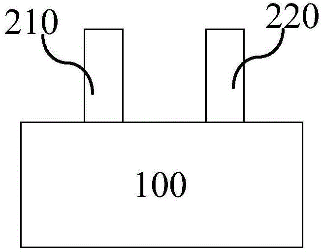
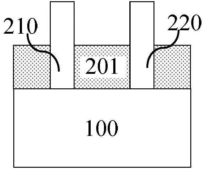
[0028] see Figure 9 , the present invention provides a FinFET structure, comprising: a substrate 100; a first fin, the first fin includes a first channel region 210 and a source region 211 located above the first channel region; a second fin sheet, the second fin is parallel to the first fin, including a second ch...


PUM


Abstract

The invention provides a FinFET structure and a manufacture method thereof. The FinFET structure comprises a substrate, a first fin, a second fin, a grid lamination layer and isolation regions, wherein the first fin comprises a first channel region and a source region placed on the first channel region and wider than the first channel region; the second fin is parallel with the first pin, and comprises a second channel region and a drain region placed on the second channel region and wider than the second channel region; the grid lamination layer covers the substrate and sidewalls of the first and second channel regions; and the isolation regions are respectively placed at the two sides of the source region and the two sides of the drain region and on the grid lamination layer to isolate the source region, the drain region and the grid lamination layer from one another. According to the invention, the new device structure is provided on the basis of a present FinFET technology, and the grid length of the device is not limited by the footprint size, and the problem caused by the short channel effects is effectively solved.

Description

technical field [0001] The present invention relates to a method for manufacturing a semiconductor device, in particular to a method for manufacturing a FinFET. technical background [0002] Moore's Law states that the number of transistors that can be accommodated on an integrated circuit doubles every 18 months, and the performance also doubles at the same time. At present, with the development of integrated circuit technology and technology, devices such as diodes, MOSFETs, and FinFETs have appeared successively, and the size of nodes has been continuously reduced. However, since 2011, silicon transistors have approached the atomic level and reached the physical limit. Due to the natural properties of this material, in addition to the short-channel effect, the quantum effect of the device also has a great impact on the performance of the device. The speed and performance of silicon transistors are hard to break through. Therefore, how to greatly improve the performance ...

Claims


Application Information

Patent Timeline
Patent Type & Authority Applications(China)
IPC IPC(8): H01L29/78H01L21/336
Inventor 李睿刘云飞尹海洲
Owner INST OF MICROELECTRONICS CHINESE ACAD OF SCI
Why Eureka
Try Eureka