Equivalent sampling device for time-delay amount automatic correction

A technology of equivalent sampling and automatic correction, which is applied in the direction of instruments, computer control, simulators, etc., can solve the problems of radar echo information loss, redundancy, equivalent sampling inhomogeneity, etc., and achieve high measurement accuracy and circuit structure Simple, real-time corrective effects

Active Publication Date: 2016-04-13
INST OF ELECTRONICS CHINESE ACAD OF SCI
7 Cites 11 Cited by

AI-Extracted Technical Summary

Problems solved by technology

[0004] Since the programmable delay chip is affected by temperature, its delay resolution will change with the change of temperature, resulting ...

Method used

In sum, the present invention automatically adjusts the amount of delay in the equivalent sampling according to the delay precision of the programmable time delay chi...

Abstract

The invention provides an equivalent sampling device for time-delay amount automatic correction. The equivalent sampling device is realized based on a programmable time-delay chip and a programmable logic gate array FPGA, wherein the time-delay amount automatic correction process comprises the steps of: utilizing the FPGA to measure the time-delay precision of the programmable time-delay chip in real time; and then according to the time-delay precision of a time-delay circuit, automatically adjusting the time-delay amount in equivalent sampling. In this way, the uniformly-spaced equivalent sampling is ensured, and the equivalent sampling device has the advantages that the circuit structure is simple, the measuring precision is high, the real-time correction capability is high, etc.

Application Domain

Technology Topic

Image

  • Equivalent sampling device for time-delay amount automatic correction
  • Equivalent sampling device for time-delay amount automatic correction
  • Equivalent sampling device for time-delay amount automatic correction

Examples

  • Experimental program(1)

Example Embodiment

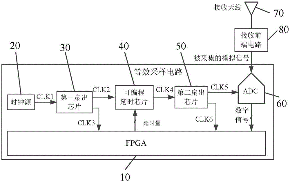
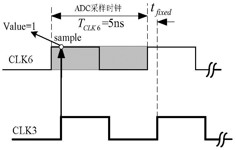
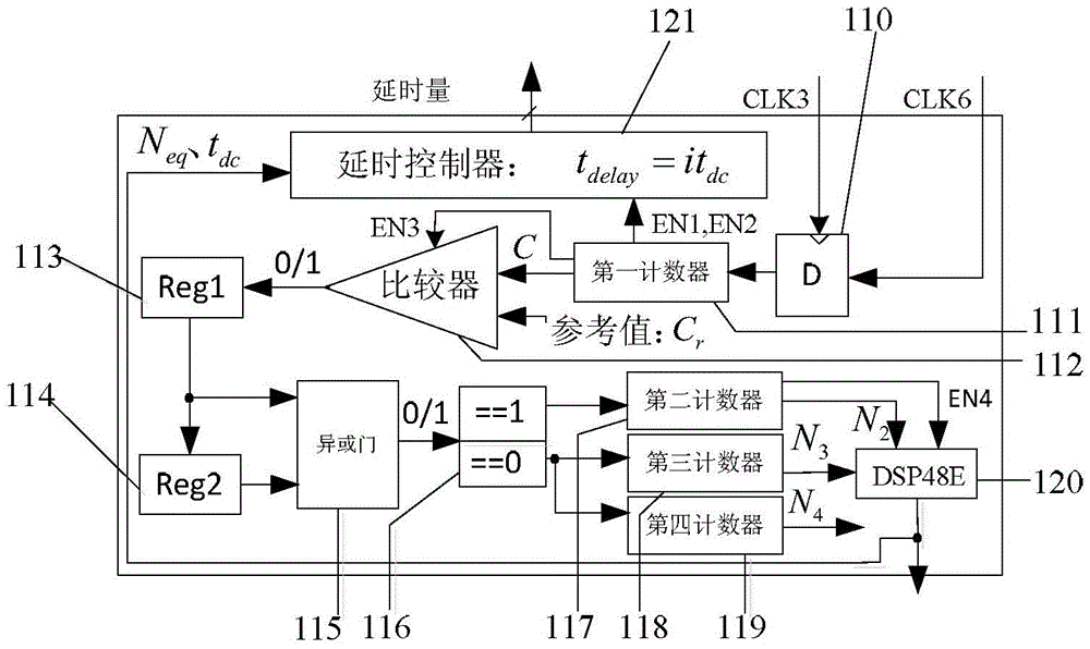
[0034] The equivalent sampling device for automatically correcting the delay amount of the present invention is based on a programmable delay chip and a programmable logic gate array FPGA, wherein the automatic correction process of the delay amount mainly includes: using the FPGA to measure the delay accuracy of the programmable delay chip in real time ; Then automatically adjust the delay amount in the equivalent sampling according to the delay accuracy of the delay circuit, so as to ensure equivalent sampling at equal intervals.
[0035] In order to make the object, technical solution and advantages of the present invention clearer, the present invention will be described in further detail below in conjunction with specific embodiments and with reference to the accompanying drawings.
[0036] In an exemplary embodiment of the present invention, an equivalent sampling device for automatic correction of delay is provided. figure 1 It is a structural schematic diagram of an equivalent sampling device for automatically correcting the delay amount according to an embodiment of the present invention. like figure 1 As shown, the equivalent sampling device of this embodiment includes:
[0037] FPGA chip 10;
[0038] A clock source 20, used to generate a stable first clock CLK1;
[0039] The first fan-out chip 30 is electrically connected to the clock source 20, and is used to generate two-way clocks-the second clock CLK2 and the third clock CLK3 by the first clock CLK1, wherein the third clock CLK3 is input to the FPGA chip 10, as its working clock;
[0040] Programmable delay chip 40, its input end is connected to the output end of the second clock CLK2 in the first fan-out chip 30, and its control end is connected to the output end of FPGA chip 10, for utilizing the time delay that this FPGA chip 10 outputs The amount delays the input second clock CLK2, generates and outputs the fourth clock CLK4;
[0041] The second fan-out chip 50 is electrically connected to the output terminal of the programmable delay chip 40, and is used to generate two clocks-the fifth clock CLK5 and the sixth clock CLK6 from the input fourth clock CLK4, wherein the sixth clock CLK6 input FPGA chip 10;
[0042] Analog-to-digital conversion chip 60, its clock input terminal is connected to the output terminal of the fifth clock CLK5 in the second fan-out chip 50, and its signal input terminal inputs an analog signal for using the fifth clock CLK5 as a sampling clock to input The analog signal is sampled and output;
[0043] Wherein, the FPGA chip 10 utilizes the third clock CLK3 as the working clock to sample the sixth clock CLK6, calculates the delay accuracy of the programmable delay chip 40, and by the delay accuracy, the time period of the first clock CLK1 and the equivalent sampling interval , generate a delay value and transmit it to the programmable delay chip 40 . Wherein, the delay precision of the programmable delay chip 40 changes with the change of the external environment temperature.
[0044] Each component of the equivalent sampling device for automatically correcting the delay amount in this embodiment will be described in detail below.
[0045] The receiving antenna 70 receives radar echo signals in the detection area. The receiving front-end circuit 80 conditions and amplifies the radar echo signal received by the receiving antenna 70 and then inputs it to the signal input terminal of the analog-to-digital conversion chip 60 . The equivalent sampling device in this embodiment performs equivalent sampling on the conditioned and amplified echo signal output by the receiving front-end circuit 80 .
[0046] The clock source 20 is a constant temperature crystal oscillator source, which provides a stable first clock CLK1 for the equivalent sampling device. Both the first fan-out chip 30 and the second fan-out chip 50 are ultra-low jitter fan-out chips. Programmable delay chip 40 provides fine step delay for equivalent sampling.
[0047] Please refer to figure 1 , the constant temperature crystal oscillator source generates a 200MHz first clock CLK1, and obtains two clocks through the first fan-out chip 3-the second clock CLK2 and the third clock CLK3, wherein the third clock CLK3 is used as the working clock of the FPGA chip, this The clock is constant. After CLK2 is delayed by the programmable delay chip 40, a fourth clock CLK4 with delay information is obtained. In order to measure the delay resolution of the programmable delay chip 40, the fourth clock CLK4 is passed through another fan-out chip to obtain two identical clocks-the fifth clock CLK5 and the sixth clock CLK6, wherein the fifth clock CLK5 is used as a module The sampling clock of the digital conversion chip ADC, and the sixth clock CLK6 is fed back to the FPGA. Now, the time difference between the third clock CLK3 and the sixth clock CLK6 includes two components: first, the delay amount t of the programmable delay chip 40 delay; Second, the fixed transmission delay t fixed. This time difference can be written as:
[0048] Δt=t delay +t fixed (1)
[0049] figure 2 It is a schematic diagram of using the sampling clock in the FPGA chip to sample the delayed sixth clock. Please refer to figure 2 , in the FPGA chip 10, the rising edge of the stable third clock CLK3 is used to sample the clock CLK6 with delay information.
[0050] image 3 for figure 1 Schematic diagram of the functional structure of the FPGA chip in the equivalent sampling device shown. refer to image 3 , the FPGA chip 10 includes:
[0051] D flip-flop 110, configured to use the third clock CLK3 as the sampling clock to sample the signal of the sixth clock CLK6;
[0052] The first counter 111, its input end is connected to the output end of D flip-flop 110, is used for accumulating the sampling times N of D flip-flop 1 And the number of occurrences C with a sampling value of 1, here set the upper limit of sampling times N ave is 512 times, when the sampling times N 1 When surpassing 512 times, this first counter 111 is cleared, and starts the time-delay setting of programmable time-delay chip 40 next time;
[0053] Comparator 112, its two input terminals input variable C and set reference value C respectively r , the control end of which is connected to the first counter 111 . When the sampling times of the first counter is equal to 512 times, the comparator 112 is enabled to determine the magnitude of the variable C and the reference value, where the reference value is set to 435. When the variable C is greater than the reference value C r When , the comparator outputs "1"; when the variable C is less than the reference value C r When , the comparator outputs "0";
[0054] The first register Reg1 and the second register Reg2 are used to register the sampling values ​​of two adjacent sixth clocks CLK6;
[0055] The XOR gate 115 performs an XOR operation on the values ​​of the two registers to obtain an XOR result. From the XOR result, it can be judged whether the rising edge or the falling edge of the sixth clock CLK6 arrives. If it arrives, the XOR result is 1 , otherwise, the XOR result is 0;
[0056] Decider 116 is used for operating the second counter 117, the third counter 118, and the fourth counter 119 according to the XOR result of the XOR gate: if the XOR result is 1, the variable N that makes the second counter 117 count 2 Increment by 1; if the XOR result is 0, and the variable N counted by the second counter 2 is 0, then make the variable N counted by the fourth counter 119 4 Self-increment by 1; otherwise, make the variable N counted by the third counter 118 3 Increment by 1;
[0057] DSP core 120 for utilizing variable N 2 and N 3 Calculate the delay resolution t of the delay chip dc , the calculation formula is:
[0058] t d c = 5 n s / N = 5 n s ( N 2 + N 3 - 1 ) - - - ( 2 )
[0059] Wherein, 5ns is the clock period provided by the first clock CLK1. When the first clock CLK1 provides the clock period t 0 When it changes, it changes with it.
[0060] At the same time, the fixed transmission delay can be calculated according to the following formula (3):
[0061] t fixed =N 4 ·t dc (3)
[0062] Delay controller 121, configured to receive the delay resolution t calculated by DSP core 120 dc , according to the delay resolution t dc Set the delay amount of programmable delay chip 40 for delay increment: t delay = it dc.
[0063] Figure 4 for figure 1 The logic flow chart of the FPGA chip measuring the delay accuracy of the delay chip in the equivalent sampling device shown. Please refer to image 3 and Figure 4 , the working process of each component in the FPGA chip includes:
[0064] (1) The D flip-flop 110 uses the third clock CLK3 as the sampling clock to sample the signal of the sixth clock CLK6;
[0065] (2) The first counter 111 accumulates the sampling times N of the D flip-flop 1 And the number of occurrences C with a sampling value of 1, judge the sampling number N of the first counter 1 Whether it reaches the set upper limit of sampling times N ave , if not, then provide the first enable signal EN1 to the delay controller 121; if so, clear the number of samples, provide the second enable signal EN2 to the delay controller 121, and provide the third enable signal to the comparator 112 EN3, output C to it;
[0066] (3) For the delay controller 121:
[0067] After receiving the first enabling signal, it keeps the delay variable i unchanged, and outputs the delay value t delay = it dc , that is, keep the current delay amount of the programmable delay chip 40;
[0068] After receiving the second enabling signal, it sets the delay variable i=i+1, and the output delay is t delay = it dc , that is, increase the delay amount of the delay chip in increments of the delay resolution;
[0069] Among them, the initial value of the delay variable i above is 0
[0070] (4) After the comparator 112 is enabled, judge the number of occurrences C and the set reference value C r relationship, such as the number of occurrences C is greater than the reference value C r When , the comparator outputs "1"; when the number of occurrences C is less than the reference value C r When , the comparator outputs "0";
[0071] (5) The value of the first register Reg1 is assigned to the second register Reg2. In the next clock cycle, the output value of the comparator is assigned to the first register Reg1. At this time, the values ​​registered in the two registers Reg1 and Reg2 are the sixth clock CLK6 Two adjacent sampling values ​​of ;
[0072] (6) Exclusive OR gate 115 performs exclusive OR operation on the output values ​​of the two registers to obtain an exclusive OR result, and then can determine the rising edge and falling edge of the sixth clock CLK6;
[0073] (7) The decision device operates the second counter 117, the third counter 118, and the fourth counter 119 according to the result of the XOR operation:
[0074] a) If the XOR result is 1, then enable the variable N counted by the second counter 117 2 Increment by 1;
[0075] b) If the XOR result is 0, and the variable N counted by the second counter 2 is 0, then enable the variable N counted by the fourth counter 119 4 Increment by 1;
[0076] variableN 4 Used to measure the fixed delay t of the sixth clock CLK6 and the third clock CLK3 fixed , the fixed delay is used to judge whether CLK6 starts to be measured.
[0077] c) otherwise, enable the variable N counted by the third counter 118 3 Increment by 1
[0078] (8) The second counter 117 judges the variable N 2 Whether it is equal to 3, if yes, if yes, then provide the fourth enable signal EN4 to DSP48E;
[0079] When the value of the second counter 117 is N 2 =3, it indicates that a complete sixth clock CLK6 has been sampled.
[0080] (9) After DSP48E receives the fourth enable signal EN4, it calculates that the total number of delays is N=N 2 +N 3 -1, the time delay resolution of the programmable time delay chip 40 calculated by using the total delay times as N is t dc =5ns/N, the delay resolution t dc sent to the delay controller.
[0081] Additionally, the number of equivalent sampling intervals to calculate Among them, [] indicates rounding up, n is a preset variable, generally an integer greater than 5 such as 8, 9 or 10, 5ns is the period of the first clock, and the number of equivalent sampling intervals is N eq sent to the delay controller.
[0082] The delay resolution of the delay chip SY89297 measured when the ambient temperature is 25°C. refer to Figure 5 , is the cumulative amount C and the reference value C of the sixth clock CLK6 r comparison. refer to Image 6 , is the result of the XOR operation of the adjacent sampling points of the sixth clock CLK6, it can be seen that the total number of delays is N=N 2 +N 3 -1=3+(1210-125-3)-1=1084, the delay resolution of the delay chip is t dc =5ns/N=4.612ps, the fixed transmission delay is t fixed =N 4 ·t dc =125*4.612ps=576.5ps.
[0083] The preset sampling interval is T s =8t dc , according to the manual of the delay chip SY89297, its delay resolution is 5ps, and it needs to be T s A total of 125 delays for the delay increment can cover the sampling clock (5ns) of an ADC. The closed-loop echo signal of the collected pseudo-random code radar is as follows: Figure 7A As shown, it can be seen that both A-scan and B-scan have periodic interference.
[0084] Using the equivalent sampling device for automatic delay correction proposed in this embodiment, if the preset sampling interval is T s =8t dc , according to the delay resolution of the measured delay chip is t dc =4.612ps, it actually needs to use the sampling interval as the delay increment for a total of Delay times, each delay increment is 36.896ps. Sampling the closed-loop echo signal of the pseudo-random coding radar such as Figure 7B As shown, it can be seen that there is no periodic interference signal in the collected A-scan and B-scan.
[0085] So far, the present embodiment has been described in detail with reference to the drawings. Based on the above description, those skilled in the art should have a clear understanding of the equivalent sampling device for automatically correcting the delay amount of the present invention.
[0086] In addition, the above definitions of each element and method are not limited to the various specific structures, shapes or methods mentioned in the embodiments, and those of ordinary skill in the art can easily modify or replace them, for example:
[0087] (1) In the drawings or in the description of the specification, the similar or identical parts all use the same figure numbers, and the implementation methods not shown or described in the drawings are forms known to those of ordinary skill in the art;
[0088] (2) While the text may provide examples of parameters including specific values, it should be understood that parameters need not be exactly equal to the corresponding values, but may approximate the corresponding values ​​within acceptable error tolerances or design constraints, which are not Affect the implementation of the present invention.
[0089]In summary, the present invention automatically adjusts the delay amount in equivalent sampling according to the delay accuracy of the programmable delay chip, ensures equivalent sampling at equal intervals, and has the advantages of simple circuit structure, high measurement accuracy, and strong real-time correction capability. advantage.
[0090] The specific embodiments described above have further described the purpose, technical solutions and beneficial effects of the present invention in detail. It should be understood that the above descriptions are only specific embodiments of the present invention and are not intended to limit the present invention. Any modifications, equivalent replacements, improvements, etc. made within the spirit and principles of the present invention shall be included within the protection scope of the present invention.

PUM

no PUM

Description & Claims & Application Information

We can also present the details of the Description, Claims and Application information to help users get a comprehensive understanding of the technical details of the patent, such as background art, summary of invention, brief description of drawings, description of embodiments, and other original content. On the other hand, users can also determine the specific scope of protection of the technology through the list of claims; as well as understand the changes in the life cycle of the technology with the presentation of the patent timeline. Login to view more.

Similar technology patents

Classification and recommendation of technical efficacy words

  • Simple circuit structure
  • High measurement accuracy

Screw rotor type surface profile error measurement instrument

ActiveCN102538700AAvoiding Probe Radius Compensation ProblemsHigh measurement accuracyUsing optical meansEngineeringHeadstock
Owner:HEFEI UNIV OF TECH

High performance direct shearing apparatus for large contact surfaces

ActiveCN102207436AHigh measurement accuracyLarge cut surface sizeUsing mechanical meansMaterial strength using steady shearing forcesShearing deformationNormal displacement
Owner:NANJING HYDRAULIC RES INST
Why Eureka
Try Eureka