
A split booster device for semiconductor equipment and its control method

A booster device and control method technology, applied in semiconductor/solid-state device manufacturing, electrical components, circuits, etc., can solve problems such as influence, uneven wafer process accuracy, etc., achieve low price, save reprocessing time, and improve process The effect of precision requirements

Active Publication Date: 2018-08-14
SHENYANG KINGSEMI CO LTD
View PDF3 Cites 0 Cited by
  • Summary
  • Abstract
  • Description
  • Claims
  • Application Information

AI Technical Summary

Problems solved by technology

[0003] Aiming at the above-mentioned deficiencies in the prior art, the technical problem to be solved by the present invention is to provide a split booster device for semiconductor equipment and its control method, which can solve the problems caused by the inhomogeneity of the air flow of the air supply system in the prior art. issues that make wafer process accuracy susceptible to

Method used


Image

  • A split booster device for semiconductor equipment and its control method
  • A split booster device for semiconductor equipment and its control method
  • A split booster device for semiconductor equipment and its control method

Examples


Embodiment Construction

[0030] The present invention will be further described in detail below in conjunction with the accompanying drawings and embodiments.

[0031] The device of the present invention is used in the air supply system of semiconductor equipment, so that the air flow in the working area can meet the process requirements required by the equipment, and achieve the purpose of effectively improving the process precision of the semiconductor wafer and saving the working time of the equipment.

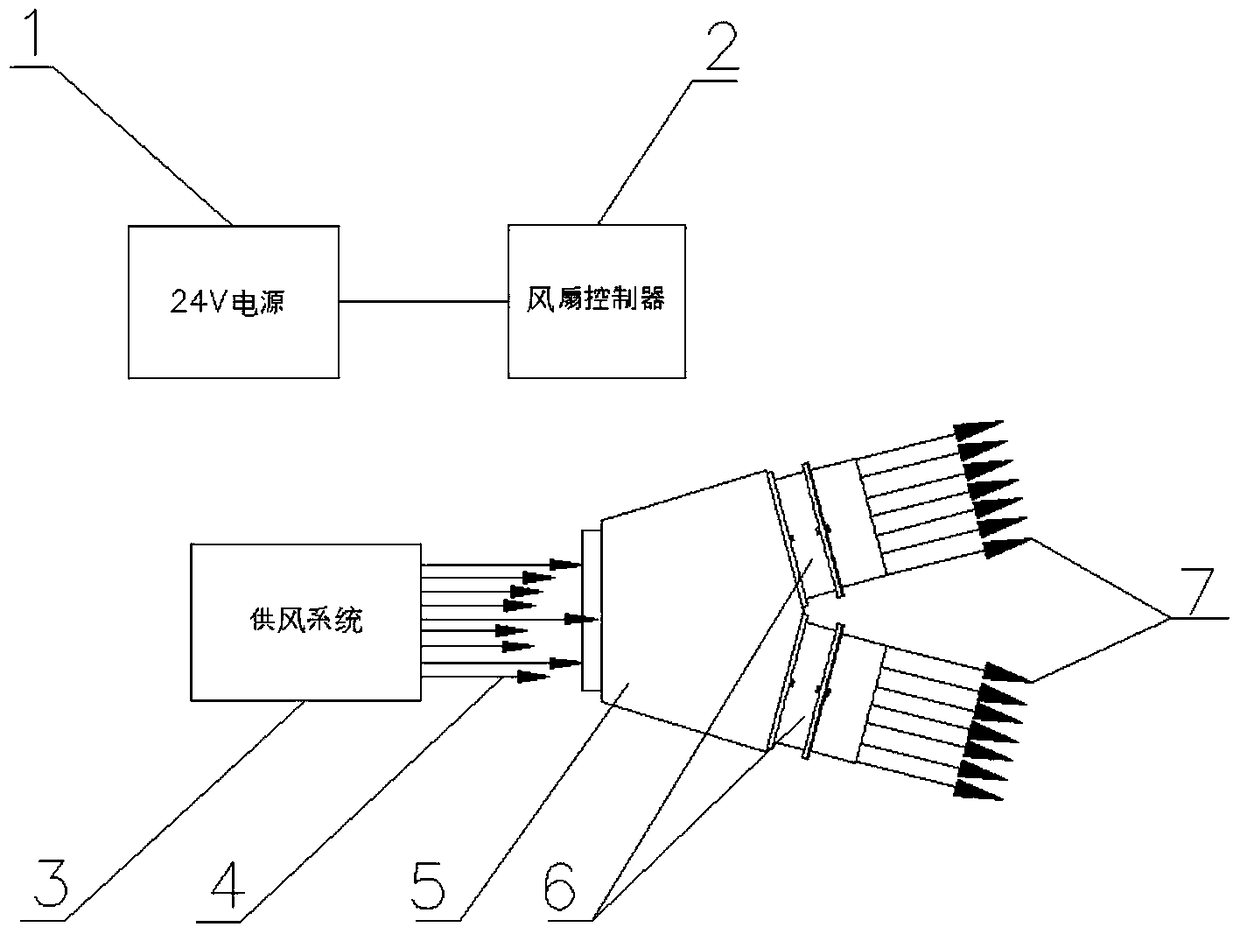
[0032] The invention is installed at the lower part of the air supply system of the semiconductor equipment. When the air supply system is working, the air duct provided is single and the air flow is uneven, which cannot meet the process requirements of wafers in the working area. The split flow supercharging device provided by the present invention can selectively adjust the speed of the electronically controlled fan according to the uneven distribution of the air supply system and the technologic...


PUM


Abstract

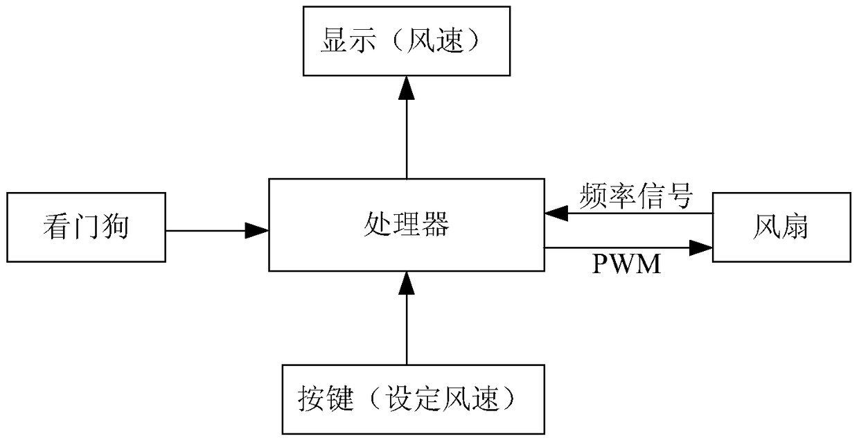
The invention relates to a shunt supercharging device for semiconductor equipment and a control method for the shunt supercharging device. The shunt supercharging device comprises an air-splitting box, electric control fans, a fan controller and a power supply, wherein an air-collecting port is aligned to an air outlet of an air supply system for shunting the air from the air outlet; air-scattering ports are connected with the electric control fans respectively; the number of the electric control fans is two, and the two electric control fans are both connected with the air-splitting box separately; the fan controller is connected with the electric control fans and used for controlling the rotating speeds of the electric control fans to further adjust air flow and uniformity; and the power supply is connected with the fan controller and used for supplying power to the fan controller. The control method comprises the steps that a set rotating speed is input through an input apparatus of the fan controller; the actual rotating speed of the electric control fans is subtracted from the set rotating speed, and inputting the difference value between the actual rotating speed and the rate rotating speed into a processor of the fan controller; and the processor of the fan controller converts the input difference value into a PWM value through PID control, and transmits the PWM value to the electric control fans. According to the control method for the shunt supercharging device, the shunt supercharging regulation is carried out through the air flow distribution of the power supply system, the uniformity of the air flow in an operating region is ensured, re-processing time is saved to a large extent, and adjustment period of equipment is reduced.

Description

technical field [0001] The invention relates to the production field of the semiconductor industry, in particular to a split booster device for semiconductor equipment and a control method thereof. Background technique [0002] In the production process of semiconductor front-end process wafers, due to the complexity and high cost of the process, the requirements for wafer production capacity and pass rate are very strict. In the actual production of semiconductor equipment, the production capacity is often reduced due to the unevenness of temperature, humidity and air flow inside the equipment, and the product qualification rate cannot be met. In the prior art, the air supply system directly exhausts the air to the working area, but the distribution and inhomogeneity of the air supply system cannot meet the requirements of the wafer process, and multiple adjustments are required, which seriously affects the working time and reduces the rate of qualified products. Contents...

Claims


Application Information

Patent Timeline
Patent Type & Authority Patents(China)
IPC IPC(8): H01L21/67
Inventor 郭聪施强
Owner SHENYANG KINGSEMI CO LTD
Learn More