Chip packaging method and chip packaging structure

A chip packaging and chip technology, which is applied in the field of chip packaging methods and chip packaging structures, can solve the problems of insulation requirements, non-adaptation, and impact on chip performance, and achieve the effects of improving flexibility, ensuring insulation, and ensuring electrical characteristics

Active Publication Date: 2016-04-13
SILERGY SEMICON TECH (HANGZHOU) CO LTD
View PDF6 Cites 3 Cited by
  • Summary
  • Abstract
  • Description
  • Claims
  • Application Information

AI Technical Summary

Problems solved by technology

[0004] However, some low-power devices do not have high requirements for heat dissipation performance, but they have very high requirements for the direct insulation between their non-active surface and PCB board, so as to prevent leakage and affect the performance of the chip.
For the packaging of this type of chip, the conventional QFN packaging method is no longer suitable.
In addition, in this conventional QFN package, it is necessary to use a prefabricated lead frame, and once the lead frame is made, the arrangement, spacing and size of the pins have been determined, which is not conducive to the flexible design of the package.

Method used


Image

  • Chip packaging method and chip packaging structure
  • Chip packaging method and chip packaging structure
  • Chip packaging method and chip packaging structure

Examples


Embodiment Construction

[0024] Hereinafter, the present invention will be described in more detail with reference to the accompanying drawings. In the various drawings, the same components are denoted by similar reference numerals. For the sake of clarity, various parts in the drawings have not been drawn to scale. Also, some well-known parts may not be shown. For simplicity, the structure obtained after several steps can be described in one figure. In the following, many specific details of the present invention are described, such as the structure, material, size, process and technique of each constituent part, for a clearer understanding of the present invention. However, the invention may be practiced without these specific details, as will be understood by those skilled in the art.

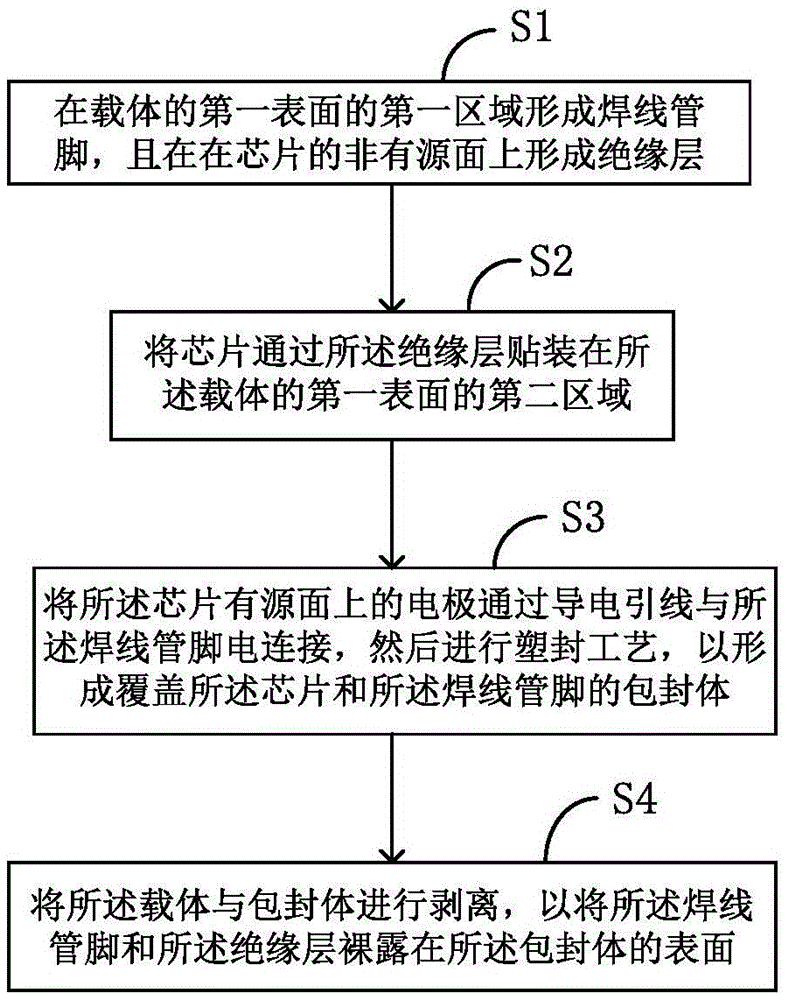
[0025] figure 1 It is a process flow diagram of a chip packaging method according to an embodiment of the present invention.

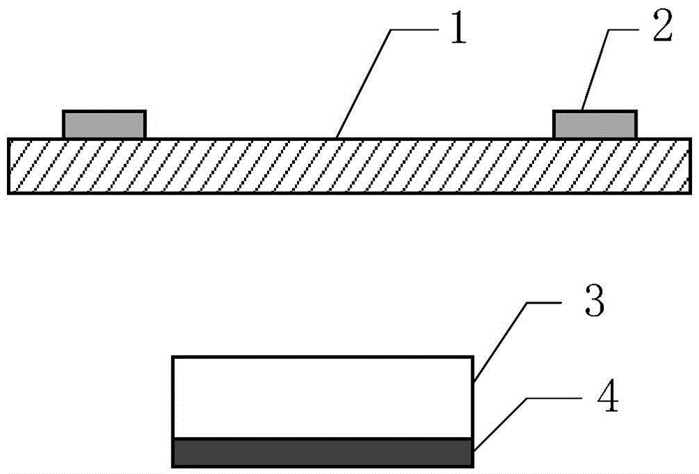
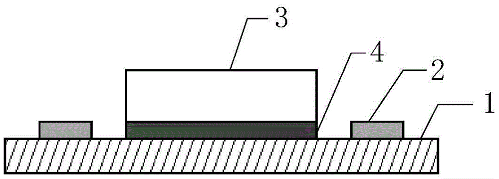
[0026] refer to figure 1 As shown, the chip method provided by the present inventi...


PUM


Abstract

The invention provides a chip packaging method and a chip packaging structure. The chip packaging method comprises the steps of forming a bonding wire pin on a first region of a carrier surface; forming an insulating layer on a non-active surface of a chip; adhering the chip to a second region of the carrier surface through the insulating layer; and after lead bonding and packaging process are completed, peeling off the carrier from a plastic packaging body to enable the insulating layer and the bonding wire pin to be exposed on the surface of the plastic packaging body. When the packaging structure formed by the packaging method is mounted on a PCB, the insulation between the non-active surface of the chip and the PCB can be ensured, and the electrical characteristic of the packaging structure is ensured as well; and in addition, according to the packaging method, a pre-fabricated lead frame is not required, instead, the bonding wire pin is formed in the packaging process, so that the flexibility of the packaging design can be improved.

Description

technical field [0001] The invention relates to the technical field of chip packaging, in particular to a chip packaging method and a chip packaging structure. Background technique [0002] The early chip package was a dual in-line DI package, which is more convenient for wiring and operation. However, the packaging efficiency of the DIP package is very low, and the area of ​​the packaged product is large, which is not conducive to increasing the capacity of the memory stick, and also affects the improvement of memory frequency, transmission rate and electrical performance. [0003] In order to reduce the packaging area of ​​the chip, surface mount technology (SMT packaging) has become a relatively popular packaging technology in the electronic assembly industry, and in SMT packaging, QFN packaging (quad flat no-lead packaging) has become the mainstream. The existing QFN packaging method is usually to install the non-active surface of the semiconductor bare chip on the midd...

Claims


Application Information

Patent Timeline
Patent Type & Authority Applications(China)
IPC IPC(8): H01L21/683H01L21/48H01L21/56H01L23/31H01L23/49
CPCH01L21/4889H01L21/56H01L21/6835H01L23/3171H01L23/49H01L23/3107H01L2224/73265H01L2224/83191H01L2224/92247H01L2924/18165H01L21/568H01L2224/48091H01L2924/00014H01L23/49506H01L23/49548H01L23/49805H01L2221/68318H01L2221/68386H01L2224/48177
Inventor 谭小春
Owner SILERGY SEMICON TECH (HANGZHOU) CO LTD
Why Eureka
Try Eureka