A Method of Saving Vdmosfet Chip Area in Low and Medium Voltage

A chip area, low voltage technology, applied in the direction of circuits, electrical components, electrical solid devices, etc., can solve the problems of increased product cost, large VDMOS area, long terminal diffusion area 6, etc., to increase the number of chip outputs and reduce Effect of chip area and cost reduction

Active Publication Date: 2016-08-17
BEIJING MXTRONICS CORP +1
View PDF7 Cites 0 Cited by
  • Summary
  • Abstract
  • Description
  • Claims
  • Application Information

AI Technical Summary

Problems solved by technology

like Image 6 As shown, the design method of the traditional VDMOS chip is as follows: form the active area 1a and the unetched area 1b by etching on the polysilicon, form the polysilicon lead area 2a on the active area 1a, and form the polysilicon on the unetched area 1b Termination structure region 2b; then form contact holes 4 and metal electrodes 5; since the polysilicon termination structure region 2b is located on the uncorroded region 1b, the formed terminal diffusion region 6 is longer, making the area of ​​VDMOS larger and the product cost Increase

Method used


Image

  • A Method of Saving Vdmosfet Chip Area in Low and Medium Voltage
  • A Method of Saving Vdmosfet Chip Area in Low and Medium Voltage
  • A Method of Saving Vdmosfet Chip Area in Low and Medium Voltage

Examples


Embodiment Construction

[0021] A kind of method of saving the VDMOSFET chip area of ​​middle and low voltage of the present invention, comprises the steps:

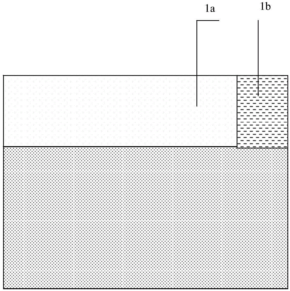
[0022] (1) if figure 1 As shown, an active region 1a and an unetched region 1b are formed by etching on polysilicon;

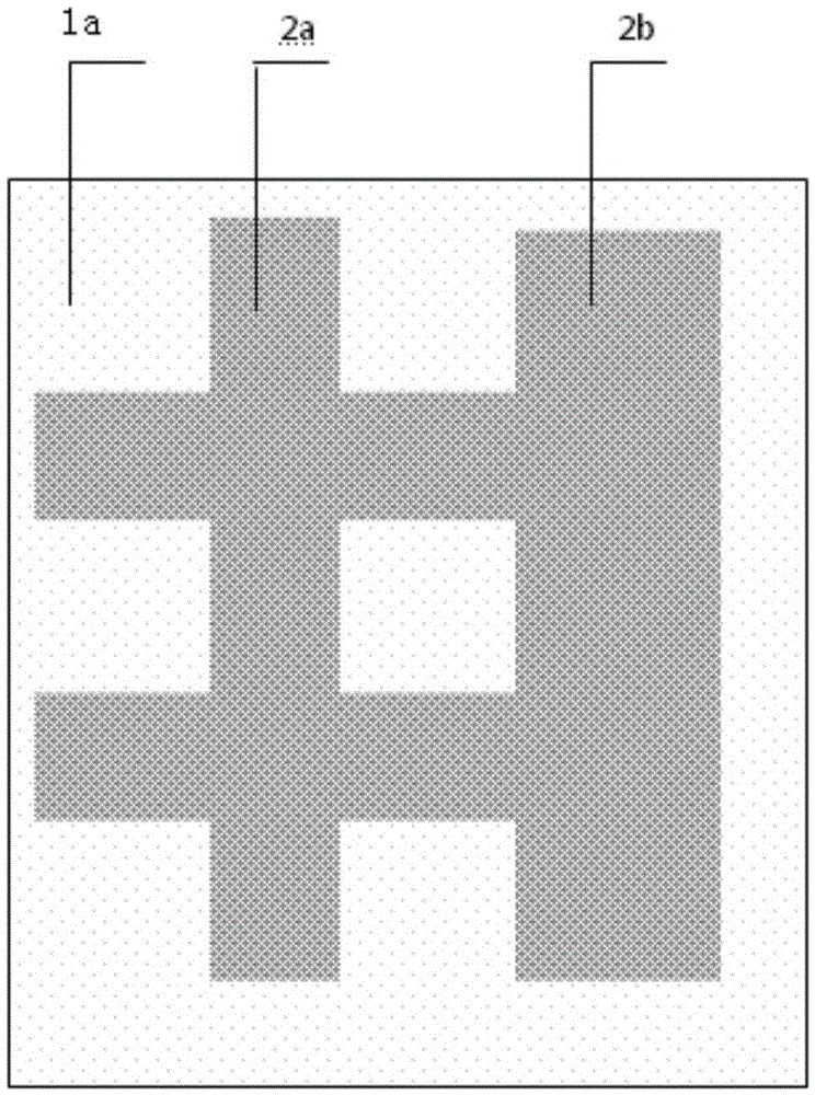
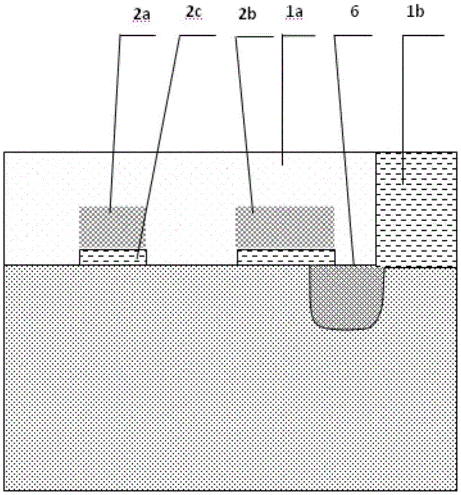
[0023] (2) As shown in Figure 2, a gate oxide region 2c and a polysilicon region 2 are formed by deposition on the active region 1a, wherein the polysilicon region 2 is located above the gate oxide region 2c; the polysilicon region 2 includes a polysilicon lead region 2a and a polysilicon region 2 Termination structure region 2b; terminal diffusion region 6 is formed by diffusion between the polysilicon termination structure region 2b and the unetched region 1b;

[0024] (3) if image 3 As shown, an N+ source region 3 is formed by diffusion under the polysilicon lead region 2a and between the polysilicon lead region 2a and the polysilicon termination structure region 2b;

[0025] (4) if Figure 4 As shown, a protective film...


PUM


Abstract

The invention discloses a method for saving the area of a medium- and low-voltage VDMOSFET chip. Electrical properties of a VDMOS device can be guaranteed, and manufacturing cost is minimized. The method comprises the following steps: firstly, an active region (1a) and a non-corrosive region (1b) are formed on polycrystalline silicon through corrosion; a polycrystalline silicon region (2) is formed on the active region (1a) through deposition, and the polycrystalline silicon region (2) contains a polycrystalline silicon lead region (2a) and a polycrystalline silicon terminal structural region (2b); N+source regions (3) are formed below the polycrystalline silicon lead region (2a) and below the space between the polycrystalline silicon lead region (2a) and the polycrystalline silicon terminal structural region (2b) through diffusion; contact holes (4) are formed on the polycrystalline silicon region; a metal electrode (5) is formed on the active region (1a); the metal electrode (5) extends to cover all the contact holes (4); the contact holes (4) are connected to the N+source regions (3) through the metal electrode (5); and the metal electrode (5) and part of the polycrystalline silicon terminal structural region (2b) are overlapped.

Description

technical field [0001] The invention relates to a design method of a VDMOSFET chip. Background technique [0002] VDMOSFET (Vertical Double Diffusion Metal Oxide Semiconductor FieldEffect Transistor, vertical conduction double diffused metal oxide semiconductor field effect transistor) chip (referred to as VDMOSFET chip or VDMOS chip) is a voltage-controlled majority carrier device. It has a series of advantages such as fast switching speed, high input impedance, low on-resistance, negative temperature coefficient, low driving power, large output power, high reliability and simple manufacturing process. It is used in DC-DC, AC-DC, automotive electronics , motor drive, industrial control, motor speed regulation, audio amplifier, high-frequency oscillator, uninterruptible power supply, energy-saving lamps, inverters and other fields have been widely used. The continuous development of power electronics technology and consumer electronics technology has opened up a wide range ...

Claims


Application Information

Patent Timeline
Patent Type & Authority Patents(China)
IPC IPC(8): H01L21/336H01L29/78
CPCH01L24/85H01L29/66712H01L29/7802
Inventor 冯幼明殷丽王成杰
Owner BEIJING MXTRONICS CORP
Why Eureka
Try Eureka