A kind of terahertz gan Gunn diode and its manufacturing method

A Gunn diode and manufacturing method technology, applied in semiconductor/solid-state device manufacturing, electrical components, circuits, etc., can solve the problems of low output power density, high device power consumption, low conversion efficiency, etc., to reduce device power consumption, The effect of improving power conversion efficiency and increasing output power density

Active Publication Date: 2018-08-17
YANGZHOU HAIKE ELECTRONICS TECH CO LTD
View PDF3 Cites 1 Cited by
  • Summary
  • Abstract
  • Description
  • Claims
  • Application Information

AI Technical Summary

Problems solved by technology

However, the InAlN electron emission layer structure in the prior art fails to solve the problems of low output power density, low conversion efficiency, and high power consumption of the device.

Method used


Image

  • A kind of terahertz gan Gunn diode and its manufacturing method
  • A kind of terahertz gan Gunn diode and its manufacturing method
  • A kind of terahertz gan Gunn diode and its manufacturing method

Examples


Embodiment Construction

[0030] In order to make the object, technical solution and advantages of the present invention clearer, the present invention will be further described below in conjunction with the accompanying drawings and specific embodiments. It should be understood that the specific embodiments described here are only used to explain the present invention, not to limit the present invention.

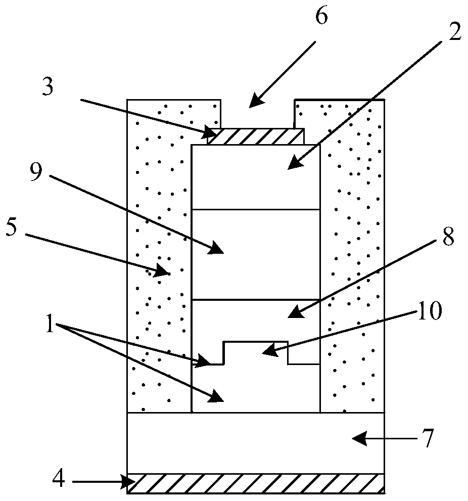
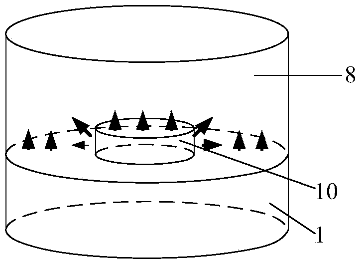
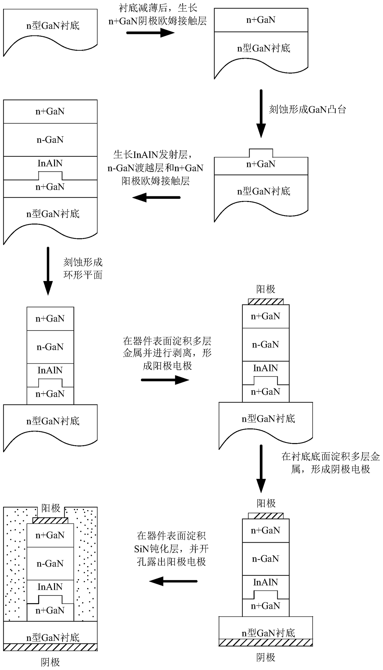
[0031] like figure 1 As shown, a terahertz GaN Gunn diode includes a cathode 4, an n-type GaN substrate 7, and an n-type GaN substrate 7 arranged in sequence from bottom to top. + GaN cathode ohmic contact layer 1, InAlN three-dimensional structure electron emission layer 8, n - GaN transition layer 9, n + The GaN anode ohmic contact layer 2 and the anode 3 also include an n-type GaN substrate 7 and wrapped around the n-type GaN substrate. + GaN cathode ohmic contact layer 1, InAlN three-dimensional structure electron emission layer 8, n - GaN transition layer 9, n + GaN anode ohmic contact lay...


PUM

PropertyMeasurementUnit
Heightaaaaaaaaaa
Diameteraaaaaaaaaa
Thicknessaaaaaaaaaa

Abstract

The invention relates to a Terahertz GaN Gunn diode and a manufacturing method thereof. The Terahertz GaN Gunn diode comprises a cathode, an n type GaN substrate, an n+ GaN cathode ohmic contact layer, an InAlN three-dimensional structure electronic emission layer, an n-GaN transition layer, an n+ GaN anode ohmic contact layer, and an anode which are successively arranged from bottom to top, and also comprises an SiN passivation layer arranged on the n type GaN substrate, and covering the n+ GaN cathode ohmic contact layer, the InAlN three-dimensional structure electronic emission layer, the n-GaN transition layer, the n+ GaN anode ohmic contact layer, and the anode; the upper portion of the SiN passivation layer is provided with an open pore exposing the anode. The Terahertz GaN Gunn diode employs a three-dimensional structure InAlN electric emission layer structure, and substantially increases the output power density of a GaN Gunn diode under a same size.

Description

technical field [0001] The invention belongs to the technical field of microelectronic devices, and in particular relates to a terahertz GaN Gunn diode and a manufacturing method thereof. Background technique [0002] Compared with traditional semiconductor materials (Si and GaAs), GaN has excellent performance in terms of frequency and output power. GaN-based Gunn diodes have shown broad application prospects in the terahertz field (100GHz-10THz). Relevant theoretical studies have predicted that GaN Gunn diodes with submicron transition layers can generate at least 200 GHz oscillation frequency, and the RF power density is at least 2 times higher than other traditional III-V compound Gunn diodes. [0003] In the traditional n+ / n / n+ Gunn device structure, electrons must travel a long distance to obtain enough energy, which limits the operating frequency of the device. In recent years, an n+ / n- / n / n+ diode structure has been proposed internationally to replace the original n+...

Claims


Application Information

Patent Timeline
IPC IPC(8): H01L29/861H01L29/06H01L21/329
CPCH01L29/06H01L29/6609H01L29/861
Inventor 李亮张瑾陈坤笪林荣
Owner YANGZHOU HAIKE ELECTRONICS TECH CO LTD
Why Eureka
Try Eureka