Method, system and program for designing power converter

a power converter and power density technology, applied in power conversion systems, instruments, computing, etc., can solve the problems of inability to accurately and quantitatively design the loss of semiconductor devices, so as to reduce the volume of the cooling unit, increase the output power density of the power converter, and accurately calculate the

Inactive Publication Date: 2007-12-06
NAT INST OF ADVANCED IND SCI & TECH
View PDF3 Cites 7 Cited by
  • Summary
  • Abstract
  • Description
  • Claims
  • Application Information

AI Technical Summary

Benefits of technology

[0047] (1) Since the semiconductor device loss can be separated into a component attributable to semiconductor device parameters and a component attributable to circuit parasitic parameters, the design coordination between the components is possible, whereby semiconductor device loss design which can make best use of characteristics of the semiconductor device becomes possible.
[0048] (2) Since the influence of the circuit parasitic parameters, which are generated in association with design of the wiring structure of the power converter, on the semiconductor device loss can be calculated quantitatively, optimal design of the power converter by means of coordinated design of the semiconductor device loss and the structure design necessary for increasing the output power density of the power converter becomes possible.
[0049] (3) Since the minimum value of the semiconductor device loss can be designed, a design for minimizing the volume of the cooling unit can be realized.
[0050] (4) The loss of a new-type semiconductor device in a research / development stage, which would be produced when the device is mounted on an actual power converter for practical use, can be accurately calculated, and virtual thermal design for the power converter can be accurately performed by use of the calculated loss. Therefore, problems involved in product development can be predicted in advance. Accordingly, problems associated with circuit and converter design can be fed back to development of semiconductor devices, whereby the efficiency of the research and development can be improved.
[0051] (5) Since virtual thermal design can be performed by making use of the designed value of the semiconductor device loss, the responsibilities of sections which share the work in the course of putting the power converter into practice can be predicted from the development stage of a new-type semiconductor device, whereby the development period can be shortened greatly, and efficient research and development becomes possible.
[0052] According to the present invention, in thermal design for a power converter, extrinsic parameters (parasitic parameters), such as parasitic inductance and parasitic capacitance, which have conventionally been ignored, and true circuit parameters and true semiconductor device parameters, which have been used in conventional design, are separated; and the influences of the true and extrinsic parameters on semiconductor device loss, filter loss, and filter frequency characteristic are calculated quantitatively. This enables comprehensive design of a power converter circuit which comprehensively realizes control design, device / main circuit design, and filter design while using extrinsic parameters as parameters. Thus, it becomes possible to easily perform optimal selection of extrinsic parameters necessary for realizing a compact, lightweight power converter of high output power density. As a result, through application of the present invention, many advantageous effects as described below, which have not been realized by conventional semiconductor device loss design methods, can be realized.

Problems solved by technology

Consequently, the parasitic inductance and the parasitic capacitance influence the loss of the semiconductor devices.
Accordingly, accurately and quantitatively designing the loss of the semiconductor device is difficult.
Since the ratio of the loss attributable to the circuit parasitic parameters to the entire loss cannot be known, difficulty encounters in designing the circuit parasitic parameters which minimize the semiconductor device loss.
Further, in conventional noise design for power converters which are driven at a relatively low switching frequency of several kHz to several 10 kHz, noise design is performed only for the switching frequency determined by the control system, and resonance frequency components generated by the parasitic inductance Ls and the parasitic capacitance Cs, which are extrinsic parameters associated with the main circuit of the converter, and deterioration of filter frequency characteristics attributable to a parasitic inductance Lfs and a parasitic capacitance Cfs, which are naturally generated when the wiring structure of the filter is realized, have been ignored.
However, the conventional power converter design method having been described with reference to FIG. 34 cannot cope with such a problem.
Therefore, accurate thermal design cannot be performed by the conventional method.
Further, since an increase is seen in the ratio of loss of a passive filter, which conventionally has not be taken into consideration in the designing step, to the overall loss of the converter, in addition to a method of designing semiconductor device loss, a method of designing passive-filter loss becomes necessary.
Therefore, when a power converter which operates at high speed and high frequency at which the influence of parasitic inductance and parasitic capacitance becomes remarkable is designed, a huge amount of time is required for trial manufacture and re-resign.
Further, a converter cannot be optimally designed by the design method in which the target specifications are attained through repetition of trial manufacture and re-design.

Method used


Image

  • Method, system and program for designing power converter
  • Method, system and program for designing power converter
  • Method, system and program for designing power converter

Examples


example 1

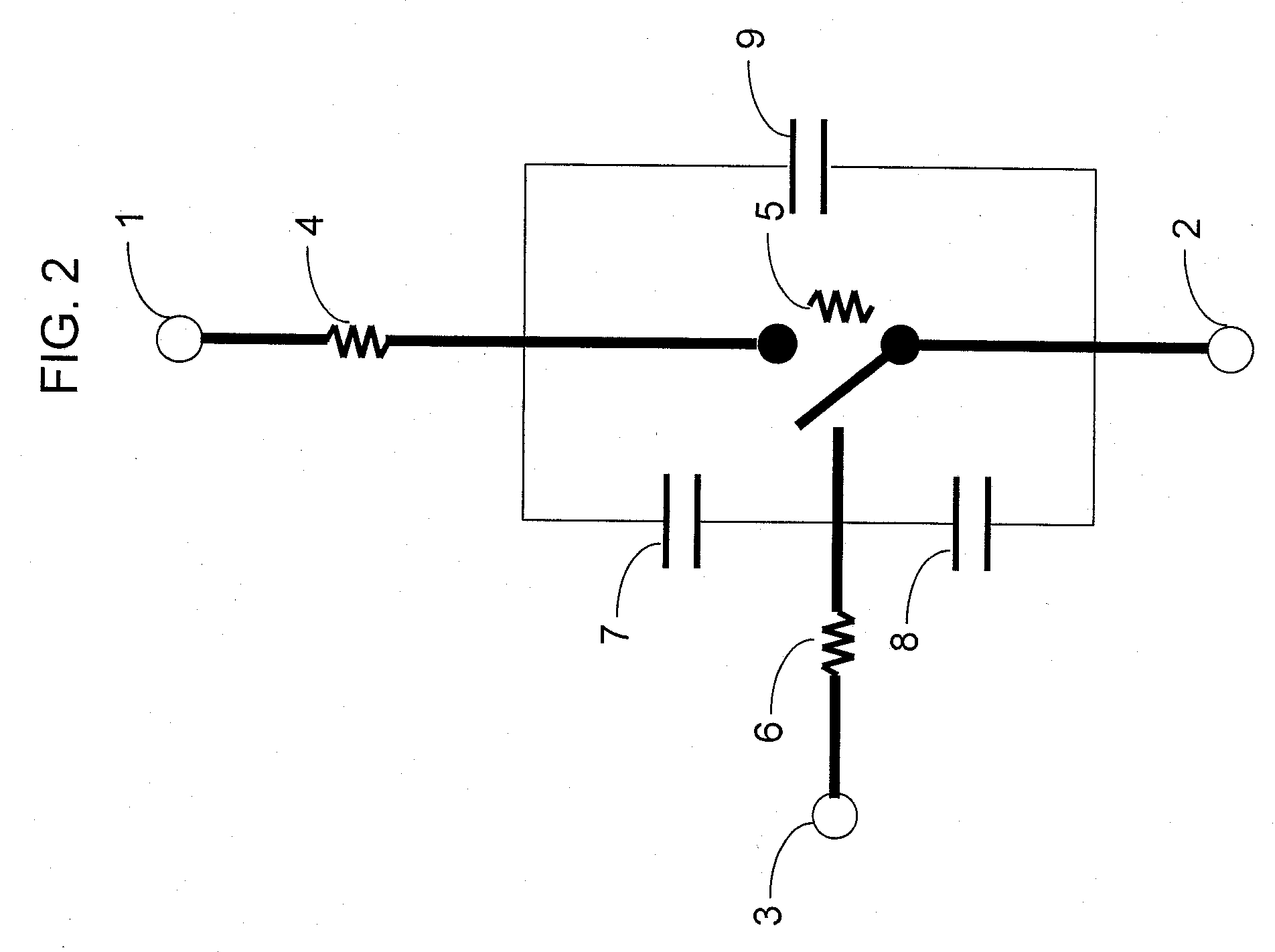
[0182]FIG. 19 is an equivalent circuit of an experimental apparatus which has a three-phase full-bridge inverter configuration and which is used for quantification of interrelations of Steps 12, 13, and 14 of FIG. 10. This experimental circuit is composed of a three-phase full bridge circuit 1, which includes semiconductor devices and a wiring structure, a passive filter 3 composed of filter inductors and filter capacitors, and a control system 4. The three-phase full bridge circuit 1, which includes semiconductor devices and a wiring structure, is formed by connecting three single-phase half bridge circuits 2 in parallel. Each of the single-phase half bridge circuits 2 is composed of semiconductor devices, circuit parasitic inductances 5, 6, and 7, circuit parasitic capacitances 8 and 9, gate inductances 10 and 11, and gate resistances 12 and 13. The circuit parasitic inductances, the circuit parasitic capacitance, the gate inductances, and the gate resistances are realized by exte...

example 2

[0185] Next, with reference to the experimental apparatus shown in FIG. 20, there will be described an example of quantification of the interrelation between the control / driver design and the device / main-circuit design which is performed in Step 12 of FIG. 10, which is a processing step for creating databases for power converter design. The semiconductor device loss and semiconductor device over-voltage greatly depend on switching frequency, switching speed, and switching pattern, which are control parameters, and circuit parasitic inductances and circuit parasitic capacitances, which are device / main-circuit parameters. The semiconductor device loss and semiconductor device over-voltage are obtained through simulation or experimentally.

[0186]FIG. 22 is an example of quantification of the interrelation between the control / driver design and the device / main-circuit design which is performed in Step 12 of FIG. 10. The semiconductor device loss was measured, while the switching frequenc...

example 3

[0187] There will be described an example of quantification of the interrelation between the device / main-circuit design and the filter design which is performed in Step 13 of FIG. 10, which is a processing step for creating databases for power converter design. The semiconductor device over-voltage greatly depends on circuit parasitic parameters, and is experimentally measured by making use of the parameter-variable circuit board of FIGS. 19, 20, and 21. Meanwhile, the filter frequency characteristic can be experimentally measured by making use of an existing measurement apparatus such as an impedance analyzer. Therefore, noise which appears on the load side as a result of passage of semiconductor device over-voltage through the filter can be experimentally measured for arbitrary circuit parameters. FIG. 23 shows the semiconductor device over-voltage for the case where the circuit parasitic inductance was changed. The horizontal axis represents the circuit parasitic inductance, and ...


PUM


Abstract

After specifications of a power converter are determined, circuit parameter values, a semiconductor device to be used, and an equivalent circuit of the semiconductor device are determined, and parameter values of the equivalent circuit are extracted. Semiconductor device loss is calculated from semiconductor device equivalent circuit parameter data, circuit parasitic parameter data, and circuit basic parameters. Determination as to whether or not the circuit loss optimal value has been achieved is made in consideration of power conversion circuit component parameter data. When the optimal value has not been achieved, the circuit parasitic parameter values are set again so as to create the circuit parasitic parameter data. When the optimal value has been achieved, the semiconductor device loss and the circuit parasitic parameter values at that time are output as design data, and the power converter is designed by use of the optimized semiconductor device loss and circuit parasitic parameter values.

Description

BACKGROUND OF THE INVENTION [0001] 1. Field of the Invention [0002] The present invention relates to a method, a system, and a program for designing a power converter. In particular, the present invention relates to a semiconductor-device-loss designing method necessary for a design which increases the output power densities of power converters. [0003] 2. Description of the Related Art [0004] Modern society depends on the premise that electrical power can be converted to a voltage, current, frequency, and phase suitable for use thereof, and electrical power can be freely used anywhere and anytime in any field of the society. Therefore, power converters, such as inverters, are used in a wide range of fields; for example, in information and telecommunication equipment, home appliances, industrial equipment, electrical railroads, power distribution systems, and power systems. With progress of power converter technologies, power converters have been reduced in size and weight. In associ...

Claims


Application Information

Patent Timeline
Patent Type & Authority Applications(United States)
IPC IPC(8): G06F19/00
CPCG06F17/5063G06F17/5036G06F30/36G06F30/367
Inventor OOHASHI, HIROMICHITAKAO, KAZUTOHAYASHI, YUUSUKE
Owner NAT INST OF ADVANCED IND SCI & TECH
Why Eureka
Try Eureka