Filling through-holes
一种铜填充、正向电流的技术,应用在液态化学镀覆、印刷元件电连接形成、涂层等方向,能够解决工人误差留下空间、效率低等问题
- Summary
- Abstract
- Description
- Claims
- Application Information
AI Technical Summary
Problems solved by technology
Method used
Image
Examples
example 1
[0036] Example 1 (comparison)
[0037] FR4 / glass-epoxy coupons 5 cm wide, 15 cm long and 200 μm thick with multiple through holes were supplied by Tech Circuit. The average diameter of the via holes is 100 μm. CIRCUPOSIT for test strips TM 880 Electroless Plating Process Plating Formulations and Methods (available from Dow Electronic Materials, Marlborough, MA) were plated to form a copper layer on one side of the coupon and on the walls of the through-holes. The thickness of the copper layer on the test piece was 0.3 μm. Pre-clean the coupons with a regular copper cleaner. The coupons were then placed in a Haring cell containing a copper electroplating bath having the formulation shown in Table 1 .
[0038] Table 1
[0039] components
quantity
copper sulfate pentahydrate
220g / L
[0040] sulfuric acid
40g / L
Chloride ions from hydrochloric acid
50ppm
polyethylene glycol
2g / L
4-Phenylimidazole / Imidaz...
example 2
[0044] Six 5 cm wide, 15 cm long and 200 μm thick FR4 / glass-epoxy coupons with multiple through holes were provided by Technical Circuits. The average diameter of the via holes is 100 μm. CIRCUPOSIT for test strips TM 880 Electroless Plating Process Plating Formulations and Methods (available from Dow Electronic Materials, Marlborough, MA) were plated to form a copper layer on one side of the coupon and on the walls of the through-holes. The thickness of the copper layer on each test piece was 0.3 μm. Pre-clean the coupons with a regular copper cleaner. The coupons were then placed in a Harlem cell containing a copper electroplating bath having the formulation as shown in Table 1 above.
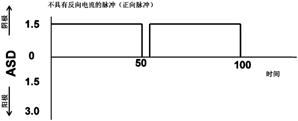
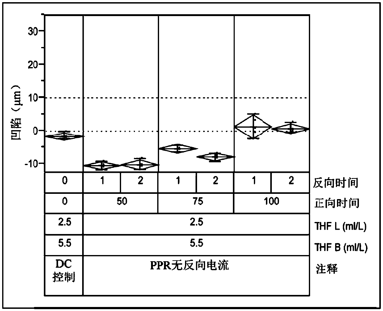
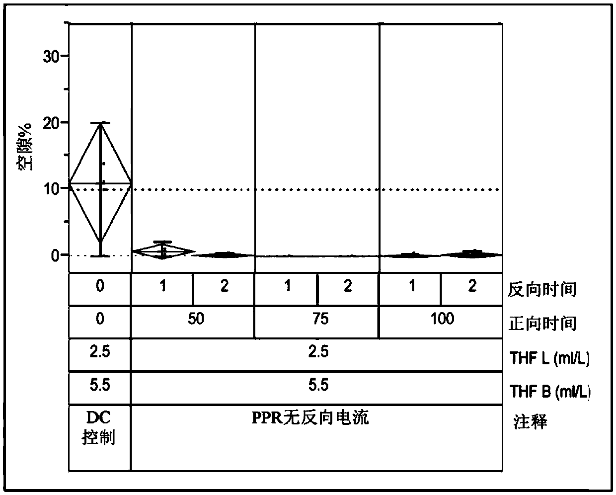
[0045] Connect the coupon to a conventional DC rectifier. The counter electrode in a Haring cell is an insoluble anode. The plating bath was air agitated at 2.4 liters / minute during electroplating. Plating was performed at room temperature. The current density was set at 1.5ASD. Two o...
example 3
[0048] The method described in Example 2 was repeated using four 5 cm wide, 15 cm long and 200 μm thick FR4 / glass-epoxy coupons with through holes having an average diameter of 100 μm. The forward pulse time is 20ms or 35ms and the break time is 1ms or 2ms. There is no reverse current. The coupons were sectioned and analyzed for dimple size and % void area as described in Example 2 above. The mean dent size of coupons plated at a forward current density for 20 ms with 1 ms current interruption was 4.3 μm and that of coupons with 2 ms current interruption was 5.4 μm. The mean dimple size for the coupons plated with a forward current density for 35 ms with a 1 ms break was -2.78 and the mean dimple size for the coupons with a 2 ms break was 6.67. All vias analyzed dropped below 10 µm. None of the coupons analyzed showed voids. In addition, no nodules were observed.
PUM
| Property | Measurement | Unit |
|---|---|---|
| diameter | aaaaa | aaaaa |
| number average molecular weight | aaaaa | aaaaa |
Abstract
Description
Claims
Application Information


