
Method of filling through-holes to reduce voids and other defects

A substrate and a predetermined time period technology, which is applied in the plating of superimposed layers, liquid chemical plating, and the formation of electrical connections of printed components, etc., can solve the problems of worker error leaving space and low efficiency

Inactive Publication Date: 2017-08-22
ROHM & HAAS ELECTRONICS MATERIALS LLC
View PDF7 Cites 3 Cited by
  • Summary
  • Abstract
  • Description
  • Claims
  • Application Information

AI Technical Summary

Problems solved by technology

Such conventional methods leave room for worker error and are inefficient

Method used


Image

  • Method of filling through-holes to reduce voids and other defects
  • Method of filling through-holes to reduce voids and other defects
  • Method of filling through-holes to reduce voids and other defects

Examples


example 1

[0044] FR4 / glass-epoxy coupons 5 cm wide, 15 cm long, and 200 μm thick with multiple through holes were supplied by Tech Circuit. The average diameter of the via holes is 100 μm. CIRCUPOSIT for test strips TM 880 Electroless Process Plating Formulation and Method (available from Dow Electronic Materials, Marlborough, Mass.) plated to form a copper layer on one side of the coupon and on the walls of the vias. The thickness of the copper layer on the test piece was 0.3 μm. Pre-clean the coupons with a regular copper cleaner. The coupons were then placed in a Haring cell containing a copper electroplating bath having the formulation as indicated in the table.

[0045] sheet

[0046] components quantity copper sulfate pentahydrate 220g / L sulfuric acid 40g / L Chloride ions from hydrochloric acid 50ppm polyethylene glycol 2g / L 4-Phenylimidazole / Imidazole / 1,4-Butanediol Diglycidyl Ether Copolymer 50mg / L (sulfopropyl)-disodium dis...

example 2

[0048] Example 2 (comparison)

[0049] FR4 / glass-epoxy coupons 5 cm wide, 15 cm long, and 200 μm thick with multiple through holes were supplied by Tech Circuit. The average diameter of the via holes is 100 μm. CIRCUPOSIT for test strips TM 880 Electroless Process Plating Formulation and Method (available from Dow Electronic Materials, Marlborough, Mass.) plated to form a copper layer on one side of the coupon and on the walls of the vias. The thickness of the copper layer on each test piece was 0.3 μm. Pre-clean the coupons with a regular copper cleaner. The coupons were then placed in a Harlem cell containing a copper electroplating bath having the formulation as shown in the table in Example 1.

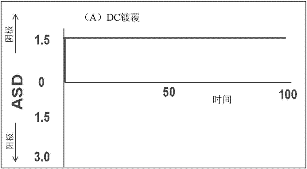
[0050] Connect the coupon to a conventional DC rectifier. The counter electrode in a Haring cell is an insoluble anode. The plating bath was air agitated at 4 liters / minute during electroplating. Plating was performed at room temperature for 63 minutes. The current density ...


PUM

PropertyMeasurementUnit
diameteraaaaaaaaaa
number average molecular weightaaaaaaaaaa

Abstract

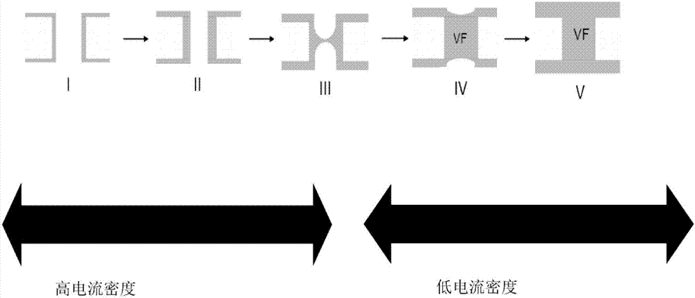
Direct current plating methods inhibit void formation, reduce dimples and eliminate nodules. The method involves electroplating copper at a high current density followed by a pause in electroplating and then turning on the current to electroplate at a lower current density to fill through-holes.

Description

technical field [0001] The present invention relates to a method of filling vias to reduce voids and other defects. More specifically, the present invention relates to a method of filling vias to reduce voids and other defects by using a high current density for a predetermined period of time, followed by pausing the current and then by applying a direct current at a low current density for a predetermined period of time. Loop fills the vias. Background technique [0002] High density interconnection is an important design in the manufacture of printed circuit boards with through holes. The miniaturization of these devices relies on a combination of thinner core materials, reduced line widths, and smaller diameter vias. The diameter of the via hole is in the range of 75 μm to 125 μm. Filling vias with copper plating has become increasingly difficult at higher aspect ratios. This produces larger voids and deeper depressions. Another problem with via filling is the way it...

Claims


Application Information

Patent Timeline
Patent Type & Authority Applications(China)
IPC IPC(8): H05K3/42
CPCH05K3/424H05K2203/0723C25D5/18C25D5/10C25D7/00C25D7/123H05K3/423H05K2203/072C25D3/38C25D5/02H05K3/0094C25D5/56C23C18/1653C23C18/38C23C28/023C25D21/12
Inventor N·嘉雅拉朱L·巴斯塔德Z·尼亚兹伊别特娃J·狄茨维斯泽柯
Owner ROHM & HAAS ELECTRONICS MATERIALS LLC
Learn More