Transistors and methods of forming them

A technology of transistors and gases, applied in the field of transistors and their formation, can solve the problems of boron ions not acting as carriers, low content of effective boron ions, and differences in transistor performance, so as to reduce the difference in distribution of P-type ions and achieve consistent performance , the effect of improving performance

Active Publication Date: 2019-01-22
SEMICON MFG INT (SHANGHAI) CORP
View PDF5 Cites 0 Cited by
  • Summary
  • Abstract
  • Description
  • Claims
  • Application Information

AI Technical Summary

Problems solved by technology

However, using the method of in-situ doping boron ions in the prior art, some boron ions cannot act as carriers, and the content of effective boron ions that can act as carriers in the stress layer is relatively low.
Moreover, the boron content at the interface at different positions of the wafer varies greatly, which makes the performance of transistors formed at different positions different.

Method used


Image

  • Transistors and methods of forming them
  • Transistors and methods of forming them
  • Transistors and methods of forming them

Examples


Embodiment Construction

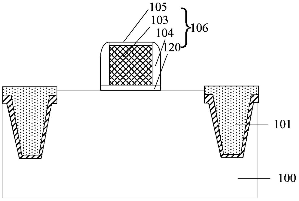
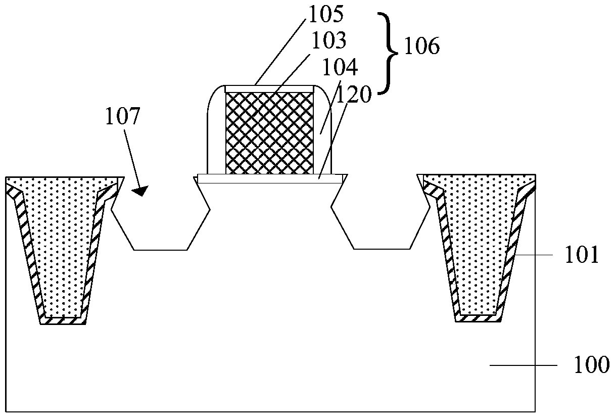
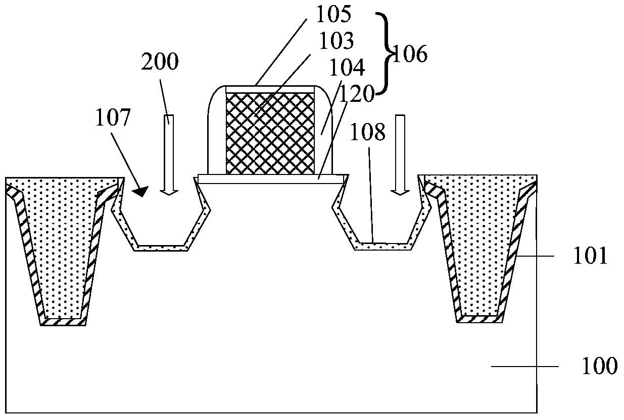
[0049] As mentioned in the background, in prior art transistors, boron ions with small atomic size tend to obtain interstitial positions at the crystal defects at the interface between the substrate and the stress layer, and gather at the interface, so that the boron ions in the stress layer The boron ion content is reduced and unevenly distributed, affecting the performance of the transistor.

[0050] Analyze the reason why boron ions are easy to gather at the interface between the substrate and the stress layer, and detect the element content of the PMOS transistor formed by the prior art. It is found that the boron ions in the stress layer are easy to diffuse to the interface, , the content of boron has an aggregation distribution shape with different peak heights. At the interface between the stress layer and the substrate, a large number of defects (lattice gaps) are generated due to lattice dislocation, and the atomic radius of boron ions is small. Trapped by defects, t...


PUM

PropertyMeasurementUnit
thicknessaaaaaaaaaa

Abstract

The invention provides a transistor and a forming method thereof. The forming method of the transistor comprises the steps as follows: a silicon substrate is provided; grooves are formed in the silicon substrate at two sides of a gate structure; a stress layer is formed in each groove; in the step of forming a stress layer, P-type doping and carbon doping are carried out to form a source and a drain; and carbon doping and P-type doping are simultaneously carried out or carbon doping is carried out before P-type doping. Carbon doped into the stress layer easily occupies a lattice space in the interface of the stress layer and the silicon substrate in priority; and when P-type ions are doped into the stress layer, the P-type ions do not easily enter the gap position on the interface of the stress layer and the silicon substrate, so that the content distribution of the P-type ions on the interface of the stress layer and the silicon substrate is improved; the effective P-type ion content in the stress layer is improved; the content distribution of the P-type ions in the stress layer is uniform; and the performance of the transistor is improved.

Description

technical field [0001] The invention relates to the field of semiconductors, in particular to a transistor and a forming method thereof. Background technique [0002] In the existing manufacturing process of semiconductor devices, improving the performance of MOS transistors through stress technology has become an increasingly common method. By appropriately controlling the stress of the channel region, the mobility of carriers (electrons in NMOS transistors and holes in PMOS transistors) can be increased, thereby increasing the driving current, thereby greatly improving the performance of the MOS transistor. [0003] At present, the embedded silicon germanium (Embedded SiGe) technology usually increases the stress of the channel region of the PMOS transistor, that is, a groove is formed in the substrate, a silicon germanium material is formed in the groove, and the source region and the source region of the PMOS transistor are formed by doping at the same time. Drain area....

Claims


Application Information

Patent Timeline
Patent Type & Authority Patents(China)
IPC IPC(8): H01L21/336H01L21/22H01L29/78H01L29/08
Inventor 周祖源
Owner SEMICON MFG INT (SHANGHAI) CORP
Why Eureka
Try Eureka