Check patentability & draft patents in minutes with Patsnap Eureka AI!

Pixel structure

一种像素结构、子像素的技术,应用在非线性光学、仪器、光学等方向,能够解决开口率低落等问题,达到高开口率的效果

Active Publication Date: 2016-05-04
AU OPTRONICS CORP
View PDF5 Cites 7 Cited by
  • Summary
  • Abstract
  • Description
  • Claims
  • Application Information

AI Technical Summary

Problems solved by technology

However, when the above-mentioned wiring method is combined with the manufacturing method in which the color filter film is directly integrated on the TFT array substrate (ColorFilteronArray, COA), it is easy to cause the problem of low aperture ratio.

Method used


Image

  • Pixel structure
  • Pixel structure
  • Pixel structure

Examples


Embodiment Construction

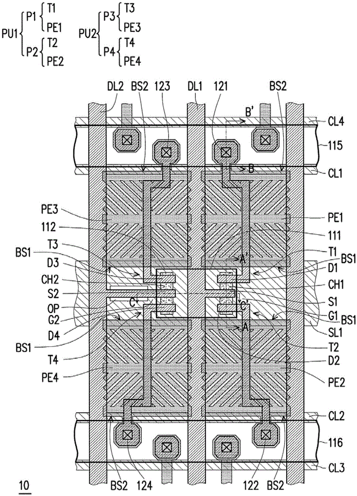
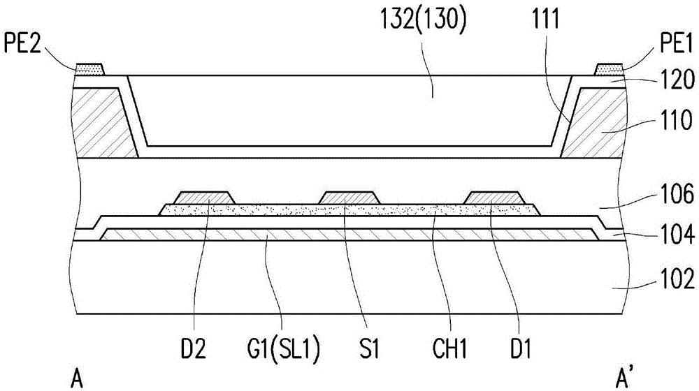
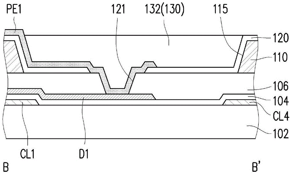
[0068] Figure 1A is a schematic diagram of a pixel structure according to an embodiment of the present invention. Figure 1B to Figure 1D are along Figure 1A Schematic cross-sectional view of lines A-A', B-B', and C-C'. Please also refer to Figure 1A to Figure 1D The pixel structure 10 includes a first scanning line SL1, a first data line DL1, a first common line CL1, a second common line CL2, a first pixel unit PU1, a color filter layer 110 and a light-shielding pattern layer arranged on the substrate 102. 130. The first data line DL1 intersects with the first scan line SL1. The first scan line SL1 is located between the first common line CL1 and the second common line CL2.

[0069] The first pixel unit PU1 includes a first sub-pixel P1 and a second sub-pixel P2. The first sub-pixel P1 includes a first active device T1 and a first pixel electrode PE1. The first active device T1 is electrically connected to the first scan line SL1 and the first data line DL1. The firs...


PUM


Abstract

The invention provides a pixel structure comprising a scanning line, a data line, a first bridging line, a second bridging line, a first sub-pixel, a second sub-pixel and a colorful filter layer. The scanning line is arranged between the first and second bridging lines; the first and second sub-pixels respectively comprise a driving element and a pixel electrode; the pixel electrode of the first sub-pixel is arranged between the scanning line and the first bridging line; the pixel electrode of the second sub-pixel is mounted between the scanning line and the second bridging line; the pixel electrode is connected with the driving element via a contact window; each pixel electrode is provided with a first side and a second side corresponding to the first side; the first side of the pixel electrode is adjacent to the scanning line; the contact window is arranged on an edge of the pixel electrode close to the second side; and the colorful filter layer is provided with an opening exposing driving elements of the first and second sub-pixels. The contact window is arranged on the edge of the pixel electrode adjacent to the bridging lines, so a problem that the light-shielding pattern falls due to excessive large size can be overcome.

Description

technical field [0001] The present invention relates to a pixel structure, and in particular to a pixel structure adapted to have smaller dimensions. Background technique [0002] With the vigorous development of display technology, the demand for display panels is gradually moving towards the direction of light and thin, high image quality, and energy saving. In particular, in order to obtain high resolution, more pixels must be laid out in the same area, so the pixel size is getting smaller and smaller, and the pixel wiring method faces more stringent challenges. [0003] Generally speaking, two common lines with different potentials are used to couple with the storage capacitors of the main sub-pixel area and the sub-sub-pixel area in the pixel structure, so that the main sub-pixel area and the sub-sub-pixel area obtain different voltages, and then Improve color cast phenomenon (colorwashout). However, when the above-mentioned wiring method is combined with the manufact...

Claims


Application Information

Patent Timeline
Patent Type & Authority Applications(China)
IPC IPC(8): G02F1/1362
CPCG02F1/1362G02F1/136209G02F1/136227G02F1/136286G02F1/136222G09G3/3607G09G2300/0426G09G2300/0443G09G2300/0452G09G3/3674G09G2320/0666
Inventor 何升儒黄孟秋白佳蕙吴尚杰陈宜瑢林弘哲
Owner AU OPTRONICS CORP
Features
  • R&D
  • Intellectual Property
  • Life Sciences
  • Materials
  • Tech Scout
  • Unparalleled Data Quality
  • Higher Quality Content
  • 60% Fewer Hallucinations
Learn More