Semiconductor apparatus manufacturing method and manufacturing apparatus

A manufacturing method and semiconductor technology, which are used in the manufacture of semiconductor devices and the field of manufacturing devices, can solve problems such as poor adhesion, inability to ensure adhesion strength, immersion, etc., and achieve the effect of preventing outflow

Active Publication Date: 2016-05-04
PANASONIC INTELLECTUAL PROPERTY MANAGEMENT CO LTD
View PDF6 Cites 6 Cited by
  • Summary
  • Abstract
  • Description
  • Claims
  • Application Information

AI Technical Summary

Problems solved by technology

If the adhesive 103 is not wetted and spreads over the entire surface of the semiconductor element 102, the adhesive strength cannot be ensured, and due to the drop impact or temperature change when the mobile device is used, poor adhesion will occur, for example, between the semiconductor element 102 and the adhesive peeling at the interface between the agent 103, or immersion of moisture from the surrounding environment, etc.

Method used


Image

  • Semiconductor apparatus manufacturing method and manufacturing apparatus
  • Semiconductor apparatus manufacturing method and manufacturing apparatus
  • Semiconductor apparatus manufacturing method and manufacturing apparatus

Examples


no. 1 Embodiment approach

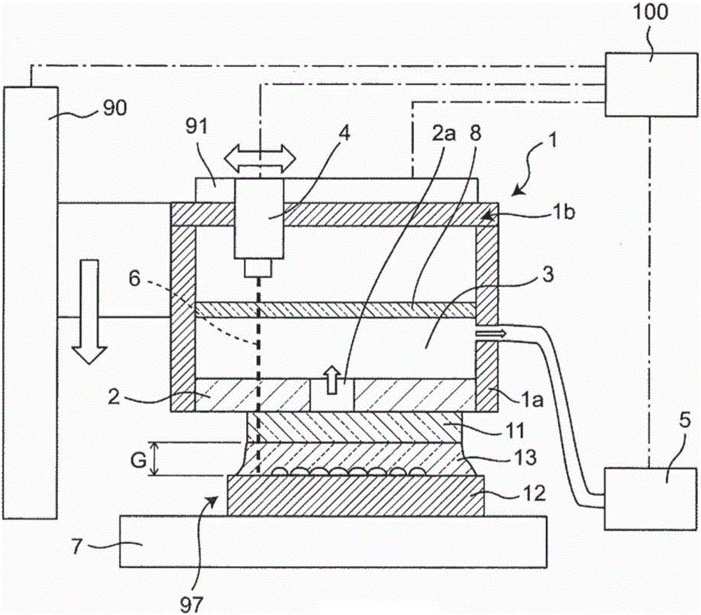
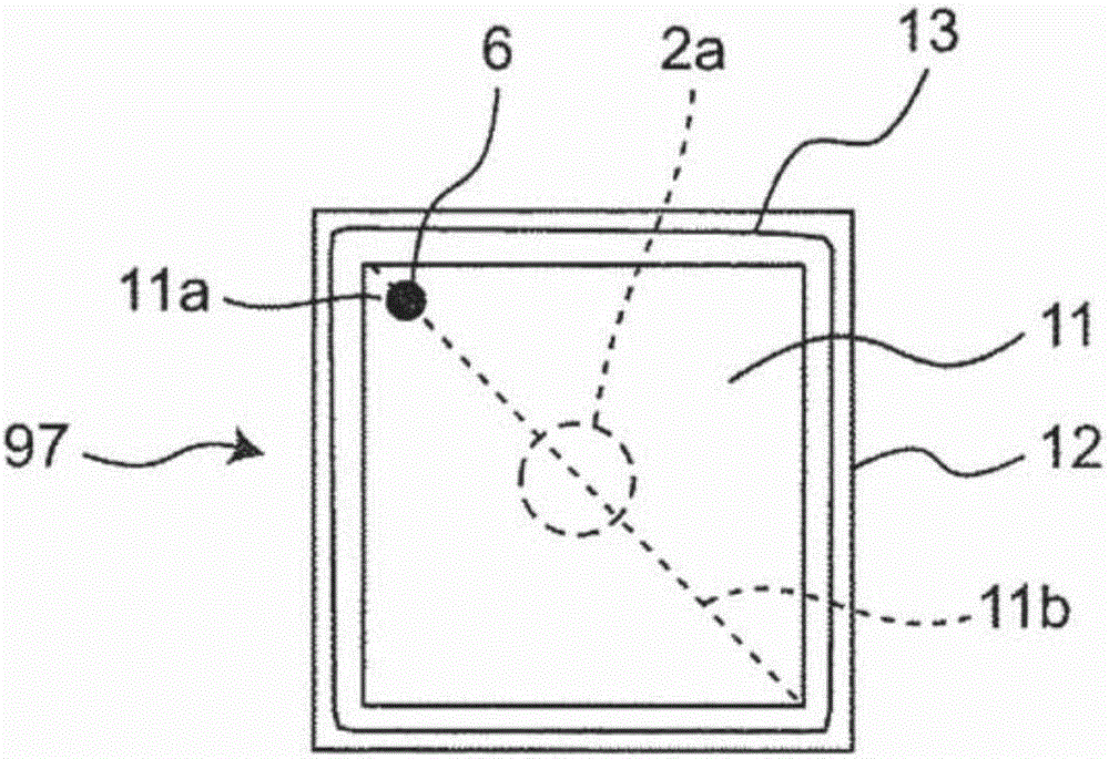
[0094] Figure 1A as well as Figure 1B It is a schematic sectional view showing the structure of the manufacturing apparatus of the semiconductor device 97 in the first embodiment of the present invention, and a plan view of the semiconductor device 97 .

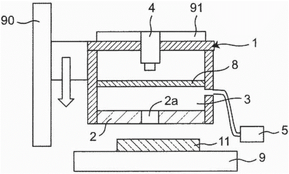
[0095] Figure 1A The semiconductor device manufacturing apparatus according to the first embodiment shown includes: a stage 7, a mounting head 1 functioning as an example of a suction tool, a mounting head drive mechanism 90, an example of a distance measuring device, and an adhesion state inspection device. An example of a device is the non-contact distance measurement mechanism 4 , the measurement mechanism drive mechanism 91 , the position information acquisition device 92 , and the control device 100 .

[0096] The stage 7 fixes the substrate 12 on which the bonding member 13 is formed.

[0097] The mounting head 1 includes a rectangular parallelepiped box-shaped main body 1 b , a transparent suction plate 2 , a tra...

no. 2 Embodiment approach

[0120] The second embodiment of the present invention differs from the first embodiment in that a mounting member 31 smaller than the mounting member 11 of the first embodiment is used; an example of a distance measuring device and an example of an adhesive state inspection device The non-contact distance measuring part 24a of the functioning non-contact distance measuring mechanism 24 is fixed, and the mirror moves; and there are two measuring positions of the laser light 26 in the inspection process.

[0121] Figure 4A ~ Figure 4F These are a schematic cross-sectional view and a plan view of the semiconductor device sequentially showing the method for manufacturing the semiconductor device in the second embodiment of the present invention.

[0122] right Figure 4A and Figure 4B The structure of the semiconductor device manufacturing apparatus of the second embodiment shown will be described. The semiconductor device manufacturing apparatus of the second embodiment incl...

no. 3 Embodiment approach

[0140] The third embodiment of the present invention has the same configuration as the semiconductor device manufacturing apparatus in the first embodiment, but differs from the first and second embodiments in that a mounting member 41 with a large warp is used, And there are four measurement locations of the laser beam 6 in the inspection process. In addition, in 3rd Embodiment, the same code|symbol is attached|subjected to the same structure as 1st Embodiment, and description is abbreviate|omitted.

[0141] The inspection process of the semiconductor device in the third embodiment will be described. Figure 5A ~ Figure 5C It is a schematic cross-sectional view and a plan view of the semiconductor device sequentially showing the manufacturing method of the semiconductor device in the third embodiment of the present invention. The steps of the following manufacturing method are also all performed under the control of the control device 100 .

[0142] First, under the control...


PUM

PropertyMeasurementUnit
Thicknessaaaaaaaaaa
Side lengthaaaaaaaaaa
Thicknessaaaaaaaaaa

Abstract

The invention provides a semiconductor apparatus manufacturing method and a manufacturing apparatus. A gap between an optical component and a base plate of a semiconductor element can be guaranteed at high precision during an installation bonding procedure for optical components; and undesirable bonding can be determined and output of undesirable bonding products to following procedures can be avoided. Detection light (6) can illuminate in an installation component (11) and a bonding component (13), so a distance between the installation component and the base plate in a vertical direction can be determined and the detection light can illuminate at least one corner side of the installation component in a transverse way along the vertical direction of the installation component when the distance between the installation component and the base plate (12) is close to a regulated distance; and a bonding state can be checked via waveform of reflection light.

Description

technical field [0001] The present invention relates to a semiconductor device manufacturing method and manufacturing apparatus for manufacturing a semiconductor device by mounting optical components such as optical glass or lenses on semiconductor elements such as solid-state imaging devices. Background technique [0002] In recent years, as electronic devices such as smartphones and tablet terminals have been miniaturized and enhanced in performance, the trend toward miniaturization and higher density of devices used in these terminals is accelerating. In such a device, the distance between the optical component and the semiconductor element, that is, the gap (gap), has a large influence on the characteristics of the device. [0003] As an example of such a device, there is an imaging device. Packaging methods for imaging devices are changing from conventional packaging methods to chip-size packaging that enables miniaturization. Among them, the conventional packaging me...

Claims


Application Information

Patent Timeline
IPC IPC(8): H01L21/00H01L21/67
CPCH01L21/00H01L21/67
Inventor 樱井大辅近藤繁三宅贵大
Owner PANASONIC INTELLECTUAL PROPERTY MANAGEMENT CO LTD
Why Eureka
Try Eureka