Area fingerprint sensor

A fingerprint sensor and area array technology, applied in the field of area array fingerprint sensors, can solve the problem of difficulty in reaching the size of the peripheral mechanism, and achieve the effects of reducing space, reducing the size of the mechanism, and reducing the cost

Active Publication Date: 2019-05-28
SHANGHAI OXI TECH
View PDF8 Cites 0 Cited by
  • Summary
  • Abstract
  • Description
  • Claims
  • Application Information

AI Technical Summary

Problems solved by technology

[0010] However, whether the driver chip 21 is figure 2 The COF module method of the chip on the film shown is still as follows image 3 The COG binding method shown is still as Figure 4 In the ASG, LTPSG, or OSG circuit mode, the area outside the pixel unit array of the area fingerprint sensor 1 is relatively large
As the requirements for the size of the peripheral mechanism increase, the size of the area outside the pixel area of ​​the area array fingerprint sensor 1 is also getting smaller and smaller. It is difficult for the area fingerprint sensor of the prior art to meet the requirement of a smaller size of the peripheral mechanism

Method used


Image

  • Area fingerprint sensor
  • Area fingerprint sensor
  • Area fingerprint sensor

Examples


Embodiment Construction

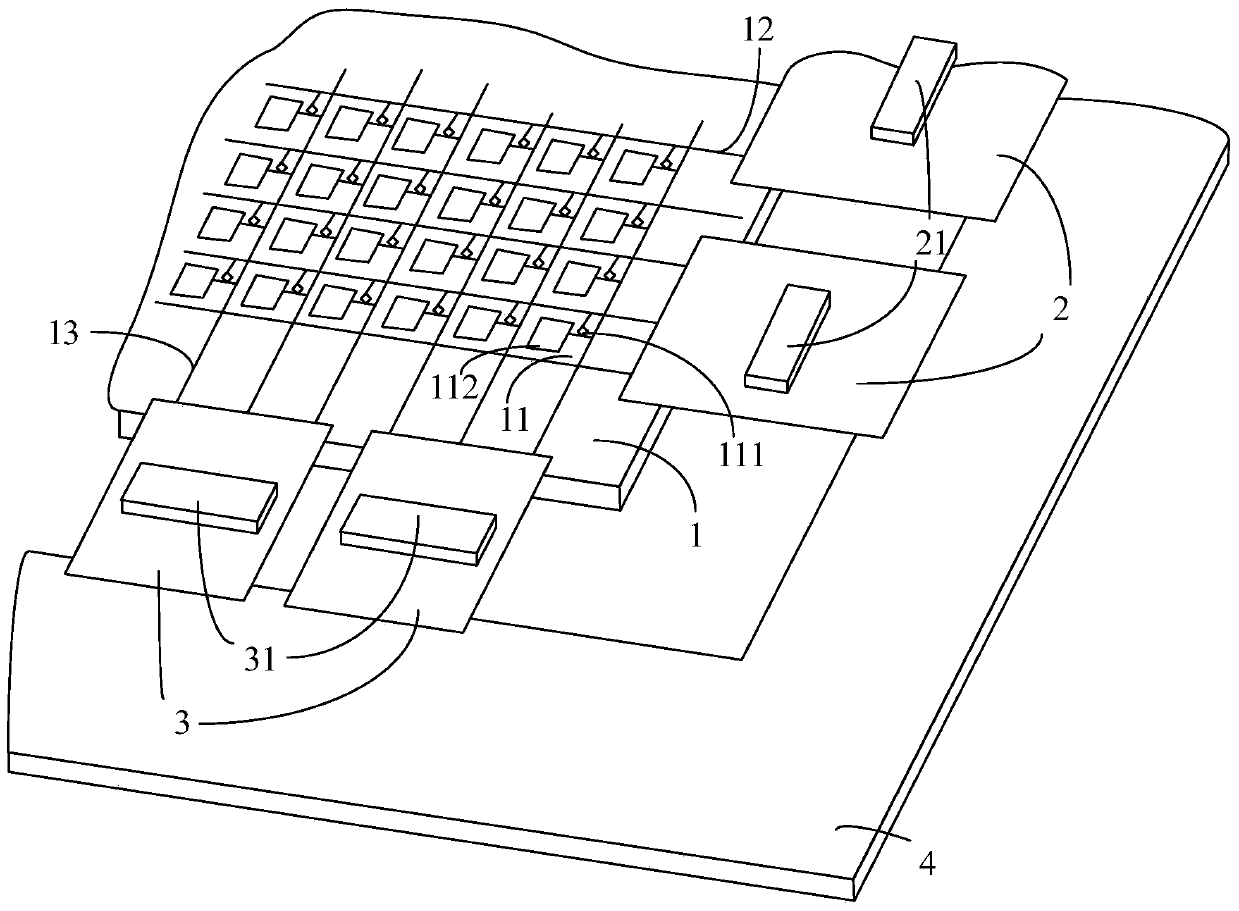
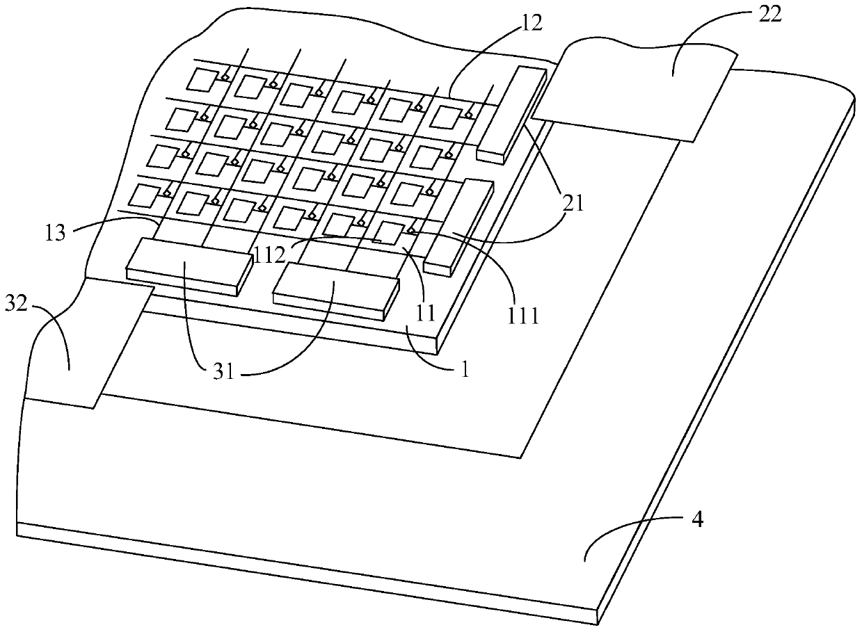
[0045] It can be seen from the background technology that in the prior art and products, whether the driver chip is figure 2 The COF module method of the chip on the film shown is still as follows image 3 The COG binding method shown is still as Figure 4 In the ASG, LTPSG, or OSG circuit mode, the area outside the pixel unit array of the area fingerprint sensor is relatively large: the driving signal input and data signal output of the pixel unit array are along the row and column directions respectively. . Correspondingly, the driving unit and the signal readout unit need to be respectively located in the row and column directions of the pixel unit array. That is to say, there needs to be enough space for setting the drive unit and the signal readout unit in both the row and column directions, thereby limiting the size of the frame of the area fingerprint sensor and restricting the reduction of the frame of the area fingerprint sensor.

[0046] In order to solve the abo...


PUM


Abstract

The invention provides an area array fingerprint sensor. The area array fingerprint sensor comprises a substrate, a pixel unit, a drive wire, a drive patch cord and a signal wire, wherein the pixel unit is arranged on the substrate like an array; the pixel unit comprises a switch device and a photoelectric device which is connected with the switch device; the photoelectric device is used for converting the optical signals with fingerprint information into electric signals; the drive wire is located on the substrate in the line direction and correspondingly connected with the switch device of the pixel unit; the drive patch cord is located on the substrate in the row direction and correspondingly connected with the drive wire and is used for transmitting an ON signal which is capable of conducting the switch device to the drive wire; the signal wire is located on the substrate along the line direction and correspondingly connected with the photoelectric device and is used for transmitting the electric signal formed by the photoelectric device. According to the area array fingerprint sensor, the peripheral mechanism size can be reduced; and moreover, the area array fingerprint sensor can be finished without changing the existing production line, so that the production cost is not increased.

Description

technical field [0001] The invention relates to the technical field of fingerprint sensing, in particular to an area array fingerprint sensor. Background technique [0002] The area fingerprint sensor is a planar imaging device, which is composed of a pixel unit array, driving lines, signal readout lines, etc. [0003] When performing fingerprint sensing, the optical signal with image information is directly projected to each pixel unit on the imaging surface of the sensor, and is absorbed by the pixel unit of the sensor to form an image. Since there is no lens or optical fiber to focus the light, it is the same size and no scaling, so there will be better imaging quality, and the imaging equipment will be thinner and lighter. [0004] refer to figure 1 , shows a schematic diagram of an area-array fingerprint sensor in the prior art. Visible light penetrating from the back is irradiated to an object close to the imaging surface of the area-array fingerprint sensor 1. The v...

Claims


Application Information

Patent Timeline
Patent Type & Authority Patents(China)
IPC IPC(8): G06K9/00G06K9/20
Inventor 凌严
Owner SHANGHAI OXI TECH
Why Eureka
Try Eureka