Crystal drive circuit

A technology for driving circuits and crystal oscillators, applied in electrical components, generating electrical pulses, pulse generation, etc., can solve problems such as increasing circuit power consumption and increasing current, and achieve the effect of improving startup speed and reducing power consumption.

Active Publication Date: 2018-02-06
SHANGHAI HUAHONG GRACE SEMICON MFG CORP
View PDF5 Cites 0 Cited by
  • Summary
  • Abstract
  • Description
  • Claims
  • Application Information

AI Technical Summary

Problems solved by technology

[0006] In the existing crystal oscillator drive circuit, in order to increase the startup speed, it is necessary to output a larger startup current in the PMOS transistor MP4, but after the startup current is increased, the current in each current path of the reference current source that provides mirror bias for the startup current will decrease. increase, which increases the power dissipation of the circuit

Method used


Image

  • Crystal drive circuit
  • Crystal drive circuit

Examples


Embodiment Construction

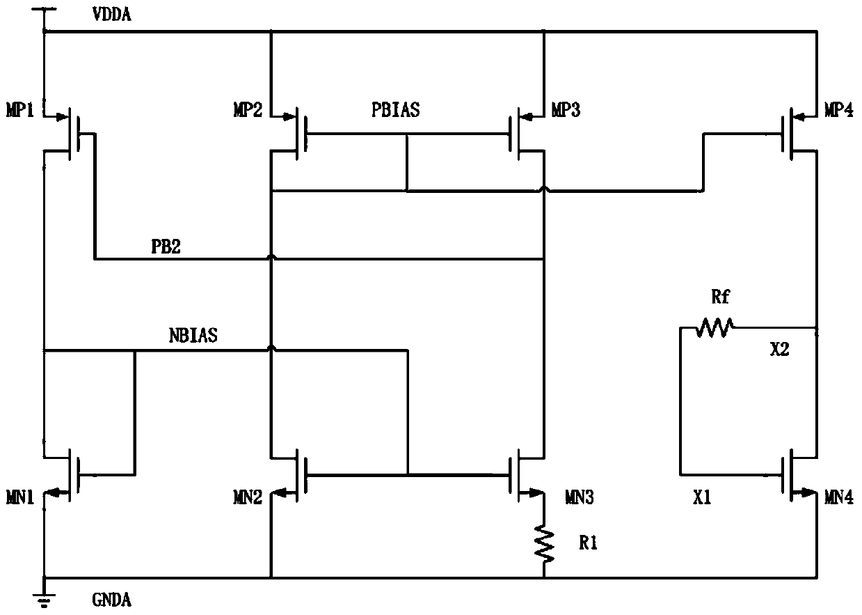
[0030] like figure 2 Shown is the crystal oscillator driving circuit diagram of the embodiment of the present invention. The crystal oscillator drive circuit provided by the present invention includes: a first current mirror, a second current mirror and an output path.

[0031] The first current mirror includes a first PMOS transistor MP1 and a second PMOS transistor MP3 that are mirror images of each other.

[0032] The second current mirror includes a first NMOS transistor MN1 and a second NMOS transistor MN3 that are mirror images of each other.

[0033] The drain current of the first PMOS transistor MP1 is connected to the drain current of the first NMOS transistor MN1 to form a first current path.

[0034] The drain current of the second PMOS transistor MP3 is connected to the drain current of the second NMOS transistor MN3 to form a second current path.

[0035] The source of the first NMOS transistor MN1 is grounded GNDA, a first resistor R1 is connected between the...


PUM


Abstract

The invention discloses a crystal oscillator drive circuit. The drive circuit comprises first and second current mirrors and an output path. The first current mirror comprises 2 PMOS tubes which mirror each other. The second current mirror comprises a first NMOS tube and a second NMOS tube, which mirror each other. The first current mirror is connected with the second current mirror, so a stable negative feedback loop is formed and reference current irrelevant to power supply voltage is output. The source electrode of the first NMOS tube is connected to the ground. A first resistor is connected between the source electrode of the second NMOS tube and the ground. The output path comprises a third PMOS tube and a third NMOS tube. The third PMOS tube and the second PMOS tube mirror each other. A feedback resistor is connected between the drain electrode and the grid electrode of the third NMOS tube. A first capacitor is connected between the grid electrode of the first NMOS tube and the grid electrode of the third NMOS tube. Before oscillation starting, the grid electrode of the first NMOST tube is provided with a direct-current bias. After the oscillation starting, an alternating-current signal of a crystal oscillator carries out an alternating-current bias on the grid electrode of the first NMOS tube. According to the invention, starting speed of the crystal oscillator can be increased and power consumption of the circuit can be reduced.

Description

technical field [0001] The invention relates to a semiconductor integrated circuit, in particular to a crystal oscillator drive circuit. Background technique [0002] Crystal oscillator drive circuits are widely used in integrated circuits, such as figure 1 Shown is the existing crystal oscillator drive circuit diagram; figure 1 The middle PMOS transistors MP1, MP2 and MP3 are mutually mirrored to form a top current mirror, and the NMOS transistors MN1, MN2 and MN3 are mutually mirrored to form a bottom current mirror, and the PMOS transistors and NMOS transistors of the top current mirror and the bottom current mirror are respectively connected to form a 3 A current path, wherein the source of the NMOS transistor MN3 and the ground are connected to the resistor R1, the sources of the NMOS transistors MN1 and MN2 are grounded; the drain and the gate of the NMOS transistor MN1 are connected to the gates of the NMOS transistors MN2 and MN3, and the connection point For node ...

Claims


Application Information

Patent Timeline
Patent Type & Authority Patents(China)
IPC IPC(8): H03K3/012
CPCH03K3/012
Inventor 邵博闻
Owner SHANGHAI HUAHONG GRACE SEMICON MFG CORP
Why Eureka
Try Eureka