Secondary-etching double-sided circuit board and processing technique thereof

A double-sided circuit board, secondary etching technology, used in printed circuits, printed circuit manufacturing, electrical components, etc., can solve the problems of uncontrolled product quality, long cycle time, and inability to meet customer requirements, and simplify production. Process and operation difficulty, the effect of reducing PCB production costs and shortening the production process cycle

Active Publication Date: 2016-05-11
苏州市三生电子有限公司
View PDF5 Cites 1 Cited by
  • Summary
  • Abstract
  • Description
  • Claims
  • Application Information

AI Technical Summary

Problems solved by technology

[0002] In the current circuit board production process, double-sided circuit boards with GTL circuit layer, GBL internal circuit layer and GBL external circuit layer are all manufactured three times, and the circuit production is completed one by one. The cumulative error of production is very large, and the product quality is not good. In terms of management and control, the operation cycle is long, the production cycle is long, the production delivery time cannot be improved, and the cost investment is also large, which cannot meet customer requirements.

Method used


Image

  • Secondary-etching double-sided circuit board and processing technique thereof
  • Secondary-etching double-sided circuit board and processing technique thereof
  • Secondary-etching double-sided circuit board and processing technique thereof

Examples


Embodiment Construction

[0026] Below in conjunction with accompanying drawing and embodiment the present invention is described in further detail:

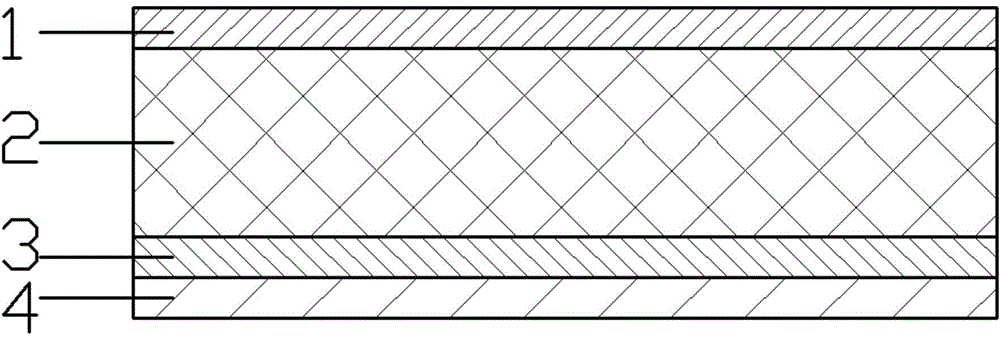
[0027] refer to image 3 As shown, a double-sided circuit board for secondary etching includes: GTL circuit layer 1, insulating PP layer 2 and GBL circuit layer, and the GBL circuit layer is composed of a GBL inner circuit layer 3 and a GBL outer circuit layer 4. The GTL line layer 1 and the GBL inner line layer 3 are connected to the insulating PP layer 2 at the same time, the GBL outer line layer 4 is covered on the GBL inner line layer 3, and the size of the GBL outer line layer 4 is larger than that of the GBL inner line layer 3 size.

[0028] The size of the GBL outer circuit layer 4 is 0.05 mm larger than the size of the GBL inner circuit layer 3 .

[0029] The secondary etched double-sided circuit board is formed through a secondary circuit processing process.

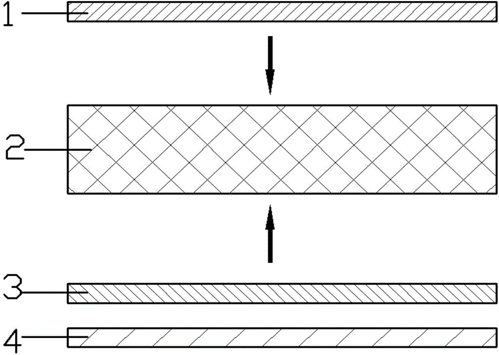
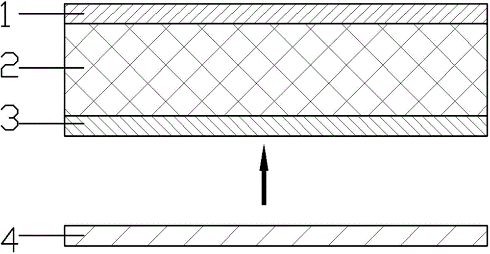
[0030] Such as figure 1 As shown, the first circuit processing technology includes...


PUM


Abstract

The invention discloses a secondary-etching double-sided circuit board and a processing technique thereof. The secondary-etching double-sided circuit board comprises a GTL line layer, an insulating PP layer and a GBL line layer. The GBL line layer is formed by a GBL inner line layer and a GBL outer line layer; the GTL line layer and the GBL inner line layer are connected with the insulating PP layer simultaneously; and the GBL outer line layer covers the GBL inner line layer. The secondary-etching double-sided circuit board is generated by a two-times circuit processing technique. The processing technique consists of a first line manufacturing process and a secondary line manufacturing process; the first line manufacturing process includes steps of first line graph manufacturing, line development, line examination, acid etching, and surface processing; and the secondary line manufacturing process includes steps of secondary line graph manufacturing, line development, line examination, etching, and electric detection on an open circuit and a short circuit, and a post procedure. According to the invention, only two-times manufacturing is carried out; the investment is low; the production flow is simplified and the working difficulty is reduced; the production efficiency is improved; the production cost is lowered; the reject ratio is reduced; and the product production period is reduced.

Description

technical field [0001] The invention relates to a circuit board, in particular to a secondary etching double-sided circuit board and its processing technology. Background technique [0002] In the current circuit board production process, double-sided circuit boards with GTL circuit layer, GBL internal circuit layer and GBL external circuit layer are all manufactured three times, and the circuit production is completed one by one. The cumulative error of production is very large, and the product quality is not good. In terms of management and control, the operation cycle is long, the production cycle is long, the production delivery time cannot be improved, and the cost investment is also large, which cannot meet customer requirements. In order to solve the above problems, a new type of superimposed circuit board circuit production update technology has been developed to improve the reliability of PCB boards, reduce PCB production costs and shorten the production process cyc...

Claims


Application Information

Patent Timeline
Patent Type & Authority Applications(China)
IPC IPC(8): H05K1/00H05K3/00
Inventor 孙祥根
Owner 苏州市三生电子有限公司
Why Eureka
Try Eureka