Automobile diode device and manufacturing method thereof

A diode and automotive technology, used in semiconductor/solid-state device manufacturing, electrical solid-state devices, semiconductor devices, etc., can solve problems such as reduced impact resistance and reliability, increased probability of contamination, and infiltration into plastic packages, and achieves consistency. Good, guaranteed reflow resistance, low cost effect

Inactive Publication Date: 2016-05-18
捷捷半导体有限公司
View PDF5 Cites 7 Cited by
  • Summary
  • Abstract
  • Description
  • Claims
  • Application Information

AI Technical Summary

Problems solved by technology

It has the advantage of adopting a split-type inner lead structure, which avoids the thickness deviation of the solder layer between the diode chip and the inner lead, but increases the process steps, increases the probability of product contamination, and increases the cost; the temperature of the solder paste for two sinterings is different, The temperature of the second sintered solder paste is close to the reflow temperature during the product application assembly process, which may cause the second sintered solder paste of the product to melt during reflow soldering and penetrate into the plastic package, resulting in the impact resistance of the product. reduction in reliability

Method used


Image

  • Automobile diode device and manufacturing method thereof
  • Automobile diode device and manufacturing method thereof
  • Automobile diode device and manufacturing method thereof

Examples


Embodiment Construction

[0030] The present invention will be further described below in conjunction with specific embodiments.

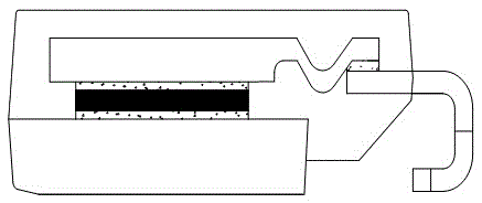
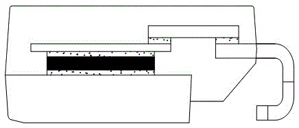
[0031] A diode device for automobiles in the present invention includes a lead frame 1, a diode chip 4, and an inner connecting piece 10 arranged in sequence. The lead frame 1 is composed of a lead frame pin 2 and a lead frame bottom plate 3. The diode chip 4 It is arranged on the lead frame bottom plate 3, and the diode chip 4 and the lead frame bottom plate 3 are connected by electrode pads A6. The inner connecting piece 10 is composed of an inner connecting piece body 5 and an inner connecting piece pin 7, so The inner connecting piece 10 is a special-shaped belt integral straight structure with upper and lower through holes 8, and the through holes 8 are on the inner connecting piece pins and above the lead frame pins 2, and the through holes 8 are A pin solder block 9 is provided, the inner connecting sheet main body 5 is arranged on the diode chip 4, and the inner connec...


PUM


Abstract

The invention relates to an automobile diode device comprising a lead framework, a diode chip, and an in-connection strap which are successively arranged. The lead framework comprises a lead framework pin and a lead framework base plate. The in-connection strap comprises an in-connection strap main body and an in-connection strap pin. Space is kept between the in-connection trap pin and the lead framework pin. The in-connection strap pin is provided with a through hole. The through hole is provided with a pin solder block therein. The space between the in-connection strap pin and the lead framework pin is filled up with the melted pin solder block in the in-connection strap through hole. The invention also relates to the manufacturing method of the diode device mentioned above. The method comprises following steps: an electrode soldering lug A, a diode chip, an electrode soldering lug B and the in-connection strap are successively mounted on the lead framework base plate; the pin solder block is put into the through hole in the in-connection strap pin; the work piece is put in a graphite smelting device and sintered; then epoxy resin encapsulating is used for product package. The diode device has advantages such as good conformity, high reliability, and strong impact resistance.

Description

Technical field [0001] The invention relates to the field of diode devices, in particular to a diode device for automobiles and a manufacturing method thereof. Background technique [0002] Automotive diode devices are protective devices for automotive electronic equipment and systems. With the high reliability requirements of automotive electronic equipment and the working mode of reverse transient high-energy shocks when automotive diode devices work, more advanced automotive diode devices are proposed. High demands. [0003] At present, the packaging of automotive diode device products mainly adopts the following methods: [0004] 1. The inner lead integrated bending structure, the structure diagram is as follows figure 1 As shown, the manufacturing process is as follows: spot solder paste on the bottom plate of the lead frame, assemble the chip, spot solder paste on the chip and the lead frame pins, assemble the inner lead, and sinter the whole at one time. It has the advantage...

Claims


Application Information

Patent Timeline
Patent Type & Authority Applications(China)
IPC IPC(8): H01L23/31H01L23/488H01L21/56
CPCH01L21/561H01L23/3114H01L23/488H01L2224/84801H01L2924/181H01L2224/40245H01L2224/32245H01L2924/00012H01L2924/00014
Inventor 吴家健李成军王成森徐洋薛治祥尹佳军
Owner 捷捷半导体有限公司
Why Eureka
Try Eureka