P‑i‑n heterojunction optoelectronic devices based on two-dimensional layer materials

A heterojunction, p-i-n technology, applied in electrical components, semiconductor devices, circuits, etc., can solve the problems of long detection band and low temperature, achieve high signal-to-noise ratio, high avalanche gain, and reduce dark current.

Active Publication Date: 2017-11-10
NANJING UNIV
View PDF5 Cites 0 Cited by
  • Summary
  • Abstract
  • Description
  • Claims
  • Application Information

AI Technical Summary

Problems solved by technology

In addition, some infrared detectors such as indium gallium arsenic have relatively long detection bands, and the disadvantage is that they need low temperature to work normally.
These detectors all have significant limitations and drawbacks

Method used


Image

  • P‑i‑n heterojunction optoelectronic devices based on two-dimensional layer materials
  • P‑i‑n heterojunction optoelectronic devices based on two-dimensional layer materials

Examples


Embodiment Construction

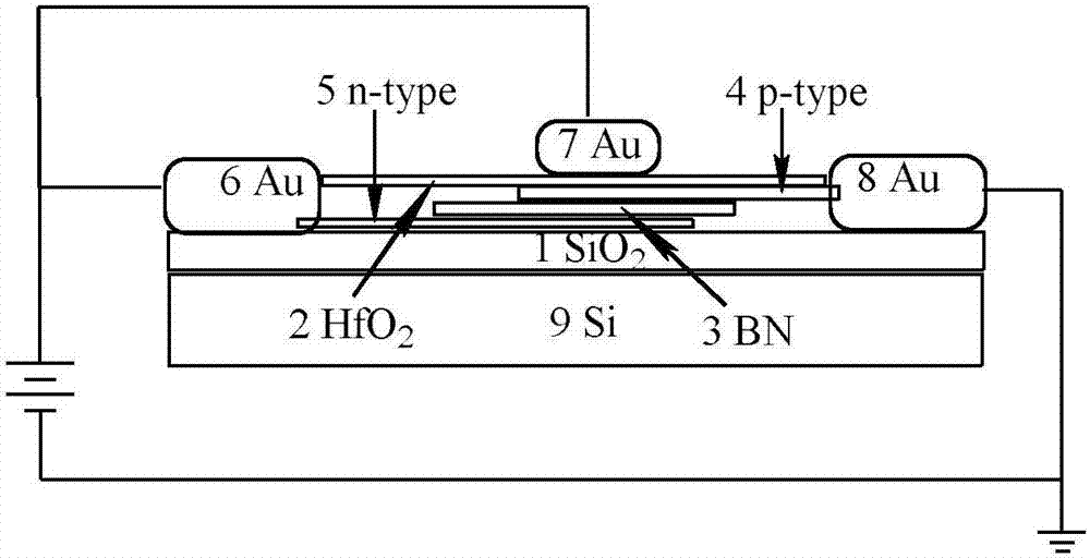
[0031] The following will clearly and completely describe the technical solutions in the embodiments of the present invention with reference to the accompanying drawings in the embodiments of the present invention. Obviously, the described embodiments are only some, not all, embodiments of the present invention. Based on the embodiments of the present invention, all other embodiments obtained by persons of ordinary skill in the art without making creative efforts belong to the protection scope of the present invention. The source electrode layer and the drain electrode layer are respectively arranged on the two semiconductor layers; the top gate electrode is arranged on the top gate dielectric layer.

[0032] The p-i-n heterojunction device includes a back gate and a top gate structure, the back gate is used to adjust the carrier concentration of the bottom semiconductor; the top gate electrode is used to adjust the carrier concentration of the top semiconductor material. The ...


PUM


Abstract

Provided is an avalanche detector based on a layered material p-i-n heterojunction. The avalanche detector comprises structures arranged on a substrate from bottom to top: a substrate insulating layer, a p-i-n heterojunction, and a top gate insulating layer, the substrate insulating layer comprises flexible insulation substrates such as silicon dioxide and PMMA, the p-i-n heterojunction comprises a p-type semiconductor two-dimensional thin film material and an n-type semiconductor two-dimensional thin film material, the p-type semiconductor two-dimensional thin film material refers to a thin film layer 5 stacked under an intrinsic semiconductor including boron nitride with large band gap and determined layer number or an insulating layer, a thin film 4 of the n-type semiconductor two-dimensional thin film material is stacked on the boron nitride, a whole heterojunction device layer is arranged on the insulating layer, the two semiconductor two-dimensional thin film material layers are separated by the boron nitride, the top gate insulating layer comprises silicon dioxide, aluminum oxide, hafnium oxide, and ITO etc., and a top gate metal electrode layer 7 is arranged on the top gate insulating layer.

Description

technical field [0001] The invention relates to the p-i-n heterojunction optoelectronic technology of two-dimensional layer-transfer materials, in particular to a p-i-n heterojunction-based optical avalanche single-photon detection. Background technique [0002] Weak photoelectron detectors have important applications in optical communication, space research and military affairs. As a highly sensitive photodetector, it can convert light signals into electrical signals, and then use it to detect the position and shape of objects. However, most of the most widely used single-photon detectors use superconducting arrays and need to work in a low-temperature environment. In particular, high-sensitivity low-light detectors have broad application requirements in the fields of cosmology research and aerospace, as well as missile guidance and quantum communication on high-end weapon platforms, which are the top priorities of research that focuses on and invests at home and abroad. ...

Claims


Application Information

Patent Timeline
Patent Type & Authority Patents(China)
IPC IPC(8): H01L31/105
CPCH01L31/105
Inventor 缪峰龙明生
Owner NANJING UNIV
Why Eureka
Try Eureka