LED chip electrode and manufacture method thereof

A technology of LED chip and manufacturing method, which is applied in the direction of circuits, electrical components, semiconductor devices, etc., can solve the problems of poor lateral expansion ability of LED chip current and the influence of LED chip luminous brightness, so as to improve horizontal expansion ability and luminous brightness , The effect of reducing manufacturing costs

Inactive Publication Date: 2016-05-18
FOCUS LIGHTINGS SCI & TECH
View PDF3 Cites 7 Cited by
  • Summary
  • Abstract
  • Description
  • Claims
  • Application Information

AI Technical Summary

Problems solved by technology

[0010] However, the current lateral expansion capability of the LED chip using the above metal electrode structure is not good, which will have a certain impact on the luminance of the LED chip.

Method used


Image

  • LED chip electrode and manufacture method thereof
  • LED chip electrode and manufacture method thereof
  • LED chip electrode and manufacture method thereof

Examples


Embodiment 1

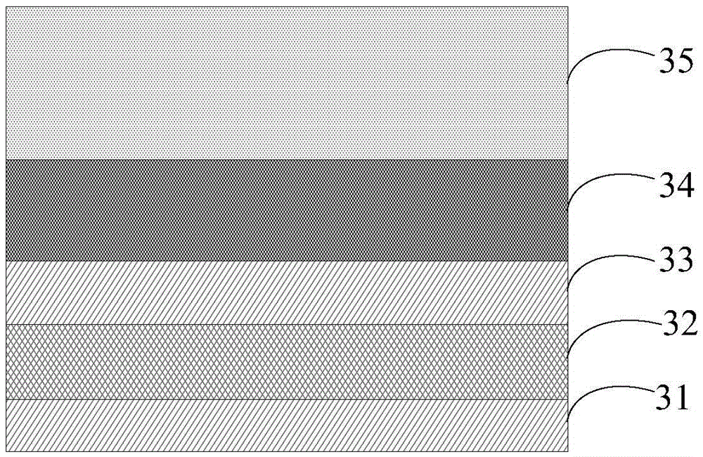
[0044] ginseng image 3 As shown, in a specific embodiment of the present invention, the LED chip electrodes sequentially include:

[0045] The first metal adhesion layer 31 is used to adhere to the semiconductor epitaxial layer and form an ohmic contact, its material is Cr, and its thickness is 5-150 Å;

[0046] The metal reflective layer 32 is used to reflect the light in the light-emitting area under the electrode to improve the luminous brightness of the LED chip. The material is Al and the thickness is 1000-3000 Å;

[0047] The second metal adhesion layer 33 is used to adhere the metal reflective layer 32 and the metal protection layer 34, and its material is Cr with a thickness of 50-500 Å;

[0048] The metal protection layer 34 is used to protect the metal reflective layer 32 and the second metal adhesion layer 33 below, and its material is Ti with a thickness of 1000-3000 Å;

[0049] The metal wiring layer 35 is used for welding the electrodes and external devices th...


PUM


Abstract

The invention discloses an LED chip electrode and a manufacture method thereof. The electrode includes a first metal adhesion layer, a second metal adhesion layer arranged on the first metal adhesion layer, a metal protection layer arranged on the second metal adhesion layer, and a metal routing layer arranged on the metal protection layer. The material of the second metal adhesion layer is the metal Cr. The material of the metal protection layer is the metal Ti. The second metal adhesion layer and the metal protection layer fuse and form a Cr-Ti contact resistor. In the electrode the metal protection layer with material of Ti is formed, the second metal adhesion layer and the metal protection layer in the electrode fuse and form the Cr-Ti contact resistor. The horizontal expansion capacity of the LED chip is effectively improved, and the luminance of an LED chip is enhanced.

Description

technical field [0001] The invention relates to the technical field of semiconductor light emitting devices, in particular to an LED chip electrode and a manufacturing method thereof. Background technique [0002] A light-emitting diode (Light-EmittingDiode, LED) is a semiconductor electronic component that can emit light. This kind of electronic component appeared as early as 1962. In the early days, it could only emit low-brightness red light. Later, other monochromatic light versions were developed. Today, the light that can be emitted has covered visible light, infrared rays and ultraviolet rays, and the brightness has also increased to a considerable level. brightness. The use has also been used as indicator lights, display panels, etc. from the beginning; with the continuous advancement of technology, light-emitting diodes have been widely used in displays, decoration and lighting. [0003] The preparation of LED chips usually includes the following steps: [0004] ...

Claims


Application Information

Patent Timeline
Patent Type & Authority Applications(China)
IPC IPC(8): H01L33/40
CPCH01L33/40H01L2933/0016
Inventor 李庆刘撰陈立人
Owner FOCUS LIGHTINGS SCI & TECH
Why Eureka
Try Eureka