Nitride light-emitting diode

A technology of light-emitting diodes and nitrides, applied in semiconductor devices, electrical components, circuits, etc., can solve the problems of high operating voltage of light-emitting diodes, large contact resistance between the P-type contact layer and the current spreading layer, and low activation efficiency of P-type impurities , to achieve the effect of improving horizontal expansion capability, reducing operating voltage, and improving antistatic performance

Inactive Publication Date: 2018-06-08
ANHUI SANAN OPTOELECTRONICS CO LTD
View PDF5 Cites 2 Cited by
  • Summary
  • Abstract
  • Description
  • Claims
  • Application Information

AI Technical Summary

Problems solved by technology

[0003] The traditional light-emitting diode structure includes a substrate, a nucleation layer, a buffer layer, an N-type GaN layer, a light-emitting layer, a low-temperature P-type GaN layer, an electron blocking layer (P-AlGaN), and a high-temperature P-type GaN layer on the substrate. , P-type contact layer, current spreading layer (such as ITO) and a pair of electrodes, the electrons provided by the N-type GaN layer and the holes provided by the P-type GaN layer recombine and emit light in the light-emitting layer, but due to the P-type GaN layer and the P-type The activation efficiency of P-type impurities (such as Mg) in the contact layer is low, and at the same time, due to the high contact resistance between the P-type contact layer and the current spreading layer, the operating voltage of the light-emitting diode is high

Method used


Image

  • Nitride light-emitting diode
  • Nitride light-emitting diode
  • Nitride light-emitting diode

Examples


Embodiment 1

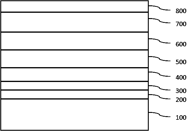
[0023] See attached figure 1 , the present invention discloses a nitride light-emitting diode, including a substrate 100, and a nucleation layer 200, a buffer layer 300, an n-type layer 400, a light-emitting layer 500, a P-type layer 600, and an N-type layer sequentially located on the substrate 100. The contact layer 700 and the current spreading layer 800 .

[0024] Traditional LEDs use Mg-doped GaN layer as the P contact layer, but the contact layer formed by the combination of Mg-doped GaN layer and current spreading layer (such as ITO) is a non-ohmic contact, and its current spreading effect is poor, making the operation of the LED High voltage, poor antistatic ability.

[0025] In the present invention, the N-type contact layer 700 is used to replace the traditional P-type contact layer. The contact layer formed in combination with the current spreading layer is an ohmic contact, and its current spreading effect is better, which reduces the risk of device breakdown due ...

Embodiment 2

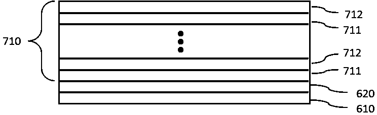
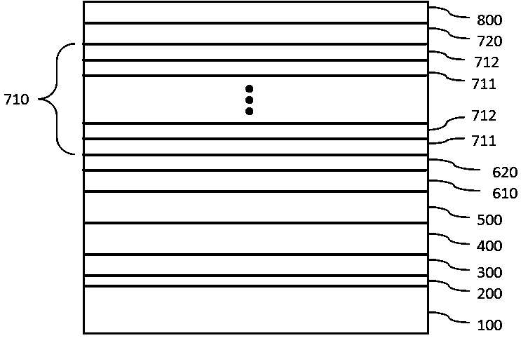
[0035] See attached image 3 , The difference between this embodiment and Embodiment 1 is that in order to further improve the contact resistance between the N-type contact layer 700 and the current spreading layer 800 on it, and the ability to expand the injection current, the u-GaN / n-GaN superlattice structure An n+ GaN layer 720 is added on the surface of the layer 710, and the n-type impurity concentration of the n+ GaN layer 720 is not less than the n-type impurity concentration in the u-GaN / n-GaN superlattice structure layer 710, and the n-type impurity concentration in the n+GaN layer 720 1×10 19 ~5×10 19 / cm 3 , the thickness of the n+ GaN layer 720 is 10Ř250Å.

[0036] Therefore, the nitride light-emitting diode proposed in this embodiment includes a substrate 100, a nucleation layer 200, a buffer layer 300, an n-type layer 400, a light-emitting layer 500, a low-temperature p-type GaN layer 610, and a substrate 100 sequentially located on the substrate 100. The p...

Embodiment 3

[0038] See attached Figure 4 , the difference between this embodiment and Embodiment 1 or 2 is: etching part of the current spreading layer 800, the N-type contact layer 700, the P-type layer 600 and the light-emitting layer 500 to the n-type layer 400 to form an n-type platform, and connect with the n-type An N electrode 410 is arranged on the platform, and a P electrode 810 is arranged on the current spreading layer 800 . When a current is injected, the electrons provided by the n-type layer 400 and the holes provided by the p-type layer 600 recombine in the light-emitting layer to emit light of a certain wavelength.


PUM


Abstract

The invention discloses a nitride light-emitting diode. The nitride light-emitting diode comprises a substrate and a nucleation layer, a buffer layer, an n-type layer, a light-emitting layer, a P-typelayer and an N-type contact layer which are sequentially arranged on the substrate, the nitride light-emitting diode is characterized in that the N-type contact layer comprises a u-GaN/n-GaN superlattice structural layer. A u-GaN/n-GaN superlattice structure or a u-GaN/n-GaN superlattice structure and an n<+> GaN layer as the N-type contact layer, the contact resistance of a current expansion layer on the N-type contact layer is reduced, the horizontal expansion capability of an injection current is improved, so that the anti-static performance can be improved, and an operating voltage is reduced.

Description

technical field [0001] The invention belongs to the field of semiconductor optoelectronic devices, in particular to a nitride light-emitting diode with an N-type contact layer. Background technique [0002] At present, light-emitting diodes (LED for short) have been widely used in two major fields of lighting and display due to their advantages of high efficiency, long life, all-solid-state, self-illumination and green environmental protection. Its gallium nitride-based light-emitting diodes have become the focus of research in industry, academia and research circles at home and abroad because of their bandgap coverage of various colors. Especially in recent years, the p-type layer structure has gradually become a research hotspot in all walks of life. [0003] The traditional light-emitting diode structure includes a substrate, a nucleation layer, a buffer layer, an N-type GaN layer, a light-emitting layer, a low-temperature P-type GaN layer, an electron blocking layer (P-A...

Claims


Application Information

Patent Timeline
Patent Type & Authority Applications(China)
IPC IPC(8): H01L33/04H01L33/14H01L33/32
CPCH01L33/04H01L33/14H01L33/32
Inventor 黄理承谢翔麟黄文宾林兓兓蔡吉明
Owner ANHUI SANAN OPTOELECTRONICS CO LTD
Why Eureka
Try Eureka