Substrate fixing method and device, semiconductor processing equipment

A fixing method and a fixing device technology, which are applied in semiconductor/solid-state device manufacturing, electrical components, circuits, etc., can solve the problems of substrate temperature uniformity, poor process quality, poor flatness, and low success rate of substrate adsorption. Achieve the effects of improving the success rate of adsorption, increasing the temperature uniformity, improving the temperature uniformity and process quality

Active Publication Date: 2020-01-03
BEIJING NAURA MICROELECTRONICS EQUIP CO LTD
View PDF5 Cites 0 Cited by
  • Summary
  • Abstract
  • Description
  • Claims
  • Application Information

AI Technical Summary

Problems solved by technology

[0007] The present invention aims to solve at least one of the technical problems existing in the prior art, and proposes a substrate fixing method and device, and semiconductor processing equipment, which can not only solve the problem of poor flatness caused by direct electrostatic chucking in the prior art. The poor substrate has a low success rate of adsorption, and it can also solve the problem of poor substrate temperature uniformity and process quality caused by mechanical fixation in the prior art

Method used


Image

  • Substrate fixing method and device, semiconductor processing equipment
  • Substrate fixing method and device, semiconductor processing equipment
  • Substrate fixing method and device, semiconductor processing equipment

Examples


Embodiment Construction

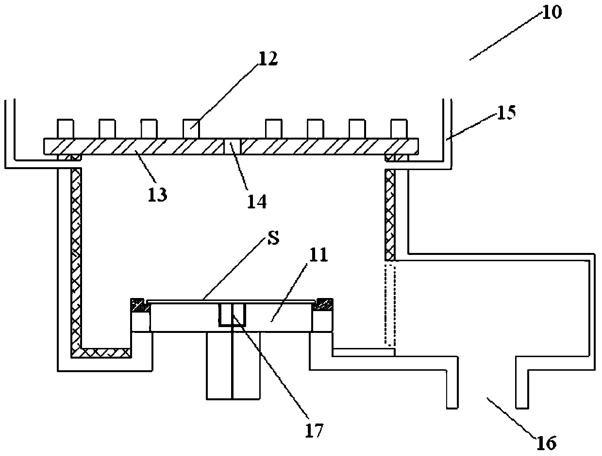
[0031] In order for those skilled in the art to better understand the technical solution of the present invention, the substrate fixing method and device, and semiconductor processing equipment provided by the present invention will be described in detail below with reference to the accompanying drawings.

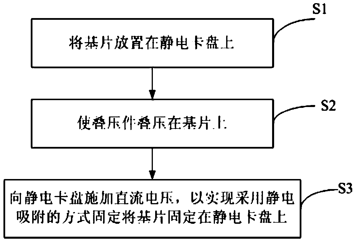
[0032] figure 2 It is a flow chart of the substrate fixing method provided by the embodiment of the present invention. see figure 2 , a substrate fixing method provided in this embodiment at least includes the following steps:

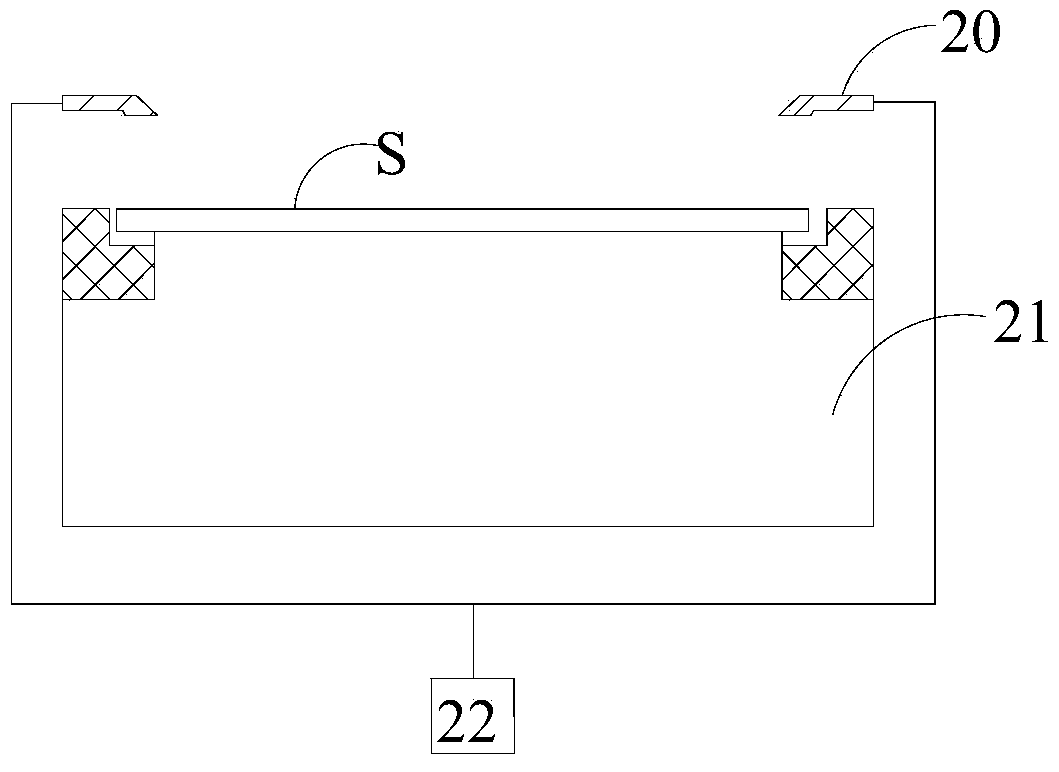
[0033] Step S1, placing the substrate on the electrostatic chuck;

[0034] Step S2, laminating the lamination on the substrate;

[0035] Step S3, applying a direct current voltage to the electrostatic chuck, so as to fix the substrate on the electrostatic chuck by means of electrostatic adsorption.

[0036]In the substrate fixing method provided in this embodiment, by means of step S2, the laminate is first laminated on the substrate, and then...


PUM


Abstract

The invention provides a substrate fixing method, a substrate fixing device and semiconductor processing equipment. The substrate fixing method at least comprises the following steps: S1, placing a substrate on an electrostatic chuck; S2, overlying an overlying element on the substrate; and S3, applying a direct voltage to the electrostatic chuck to fix the substrate to the electrostatic chuck through electrostatic adsorption. By using the substrate fixing method, the substrate fixing device and the semiconductor processing equipment provided by the invention, the problem that absorption of a substrate of poor smoothness by use of an electrostatic chuck directly is of low success rate in the prior art and the problem that the substrate temperature uniformity and process quality are poor due to the adoption of a mechanical fixing mode in the prior art are solved.

Description

technical field [0001] The invention belongs to the technical field of microelectronic processing, and in particular relates to a substrate fixing method and device, and semiconductor processing equipment. Background technique [0002] Etching equipment is one of the important equipment required in the manufacturing process of integrated circuits, which is used to complete the etching process on the substrate. [0003] figure 1 It is a schematic diagram of the structure of the reaction chamber of a typical etching equipment. see figure 1 , the reaction chamber 10 includes an electrostatic chuck 11, a coil 12, an air intake device, an exhaust device, a thimble lifting mechanism, and the like. Wherein, the electrostatic chuck 11 is arranged at the bottom of the reaction chamber 10 for fixing the substrate S on the upper surface thereof by means of electrostatic adsorption. The coil 12 is arranged above the dielectric window 13 on the top of the reaction chamber 10, and is ...

Claims


Application Information

Patent Timeline
Patent Type & Authority Patents(China)
IPC IPC(8): H01L21/683H01L21/3065
Inventor 管长乐
Owner BEIJING NAURA MICROELECTRONICS EQUIP CO LTD
Why Eureka
Try Eureka