Device for automatically detecting two-dimensional shape of wafer substrate

An automatic detection and substrate technology, applied in the direction of measuring devices, optical devices, instruments, etc., can solve problems such as laser output power and wavelength instability, and achieve the effect of improving internal heat dissipation performance and enhancing stability

Active Publication Date: 2016-06-01
北京艾瑞豪泰信息技术有限公司
View PDF8 Cites 1 Cited by
  • Summary
  • Abstract
  • Description
  • Claims
  • Application Information

AI Technical Summary

Problems solved by technology

For example, when N is 5, the specifications of the required laser are 4mm in diameter and 10mm in length, and the output power and wavelength of such a laser are unstable

Method used


Image

  • Device for automatically detecting two-dimensional shape of wafer substrate
  • Device for automatically detecting two-dimensional shape of wafer substrate
  • Device for automatically detecting two-dimensional shape of wafer substrate

Examples


Embodiment 1

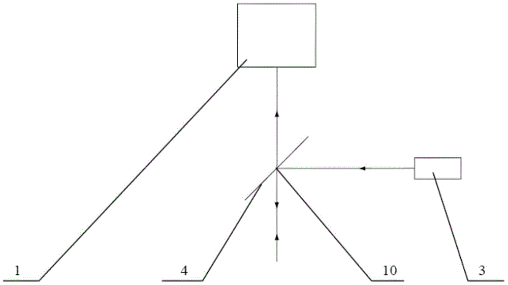
[0028] For ease of understanding, the attached figure 1 The light path diagram of only one of the spots is given.

[0029] see attached figure 1 The device for real-time and rapid detection of the two-dimensional topography of the wafer substrate provided by Embodiment 1 of the present invention includes N PSD1, N beams of laser light and the first light splitting element 4, and the N beams of laser light are arranged along a straight line, wherein N is a natural number greater than 3 , N PSD1s are in one-to-one correspondence with N laser beams,

[0030] N beams of laser light are first directed at positions 10 of the first light-splitting element 4, and incident light is formed after passing through the first light-splitting element 4, and the incident light is incident on the wafer substrate, and N incident points are formed radially on the wafer substrate, and the incident light N beams of the first type of reflected light beams are formed after being reflected by the su...

Embodiment 3

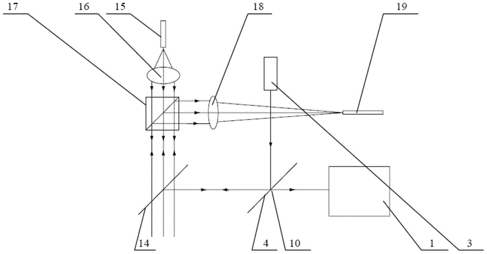
[0067] The difference between the device for real-time and rapid detection of the two-dimensional topography of the wafer substrate provided by the third embodiment of the present invention and the first and second embodiments of the present invention is that the device for the real-time rapid detection of the two-dimensional topography of the wafer substrate provided by the third embodiment of the present invention It may also include a light-passing device, which is arranged on the optical path where the incident light and the first reflected light beam pass through together. The light-passing device is provided with N light-passing holes, and the N light-passing holes correspond to the N beams of laser light one by one. , the optical holes are provided with reflective mirrors 11 at intervals, which are used to reverse the direction of the corresponding passing beam by 90°, so that the corresponding PSD can be turned to another direction, saving the placement space.

[0068] ...


PUM


Abstract

The invention discloses a device for automatically detecting the two-dimensional shape of a wafer substrate and belongs to the semiconductor material nondestructive detection technical field. In the device, a plurality of paths of emergent light of N laser beams are emitted by one laser and pass through a beam splitting prism including a plurality of beam splitting surfaces; the light intensities of the plurality of paths of emergent light emitted out from the beam splitting prism can be identical through endowing different reflectivity and transmissivity for the plurality of beam splitting surfaces, namely, the plurality of paths of emergent light with the same light intensity are not emitted by a plurality of lasers, but are obtained through reflecting and refracting the light emitted by one laser by means of the beam splitting prism, and therefore, in a limited arrangement space, a large-sized laser can be selected; when the size of the laser is increased, the inner heat dissipation performance of the laser can be improved; a feedback circuit is additionally arranged in the laser, the internal parameters of the laser can be changed according to needs; and thus, the output power and wavelength stability of the laser can be enhanced.

Description

technical field [0001] The invention relates to the technical field of non-destructive testing of semiconductor materials, in particular to a device for automatically detecting the two-dimensional shape of a wafer substrate. Background technique [0002] The invention patent application with the application number 201410188236.2 relates to a device for automatically detecting the two-dimensional shape of the wafer substrate, including N PSDs, N beams of laser light and a first beam splitting element, the N beams of laser light are arranged along a straight line, wherein the N is a natural number greater than 3, and the N PSDs correspond to N beams of laser light one by one. The N beams of laser light first shoot to the first light splitting element, and form incident light after passing through the first light splitting element. The incident light The light is incident on the wafer substrate, and N incident points are formed in the radial direction on the wafer substrate, an...

Claims


Application Information

Patent Timeline
Patent Type & Authority Applications(China)
IPC IPC(8): G01B11/245
Inventor 刘健鹏张立芳黄文勇桑云刚张瑭
Owner 北京艾瑞豪泰信息技术有限公司
Why Eureka
Try Eureka