Semi-automatic alignment and exposure device of printed circuit board (PCB)
An exposure device and PCB board technology, applied in the field of exposure machines, can solve the problems of low alignment efficiency, low alignment accuracy, and inaccurate alignment, and achieve high alignment efficiency, accurate alignment, and improved efficiency. Effect
Inactive Publication Date: 2016-06-01
永天机械设备制造(深圳)有限公司
View PDF7 Cites 6 Cited by
- Summary
- Abstract
- Description
- Claims
- Application Information
AI Technical Summary
Problems solved by technology
[0002] The PCB board needs to be aligned before exposure. The existing alignment device is manually aligned. There are some differences in this alignment. For example, the alignment between the PCB board and the film is observed by human eyes during alignment. In this case, the alignment error is relatively large, the alignment accuracy is not high, and the alignment efficiency is relatively low. At the same time, due to the inaccurate alignment, the pass rate of the PCB board is relatively low after the PCB board is exposed.
Method used
View moreImage
Smart ImageViewing Examples
Examples
no. 2 example
[0032] In the second embodiment, the difference between this embodiment and the first embodiment is that the LED lamp emits light at a certain angle to the first workbench or the second workbench.
Login to View More PUM
 Abstract
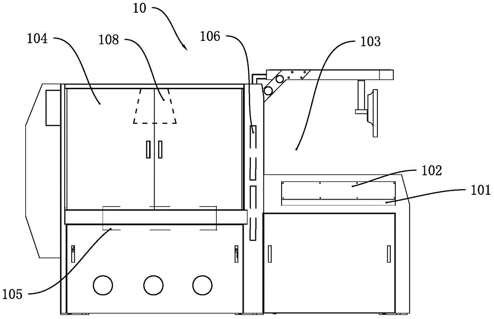
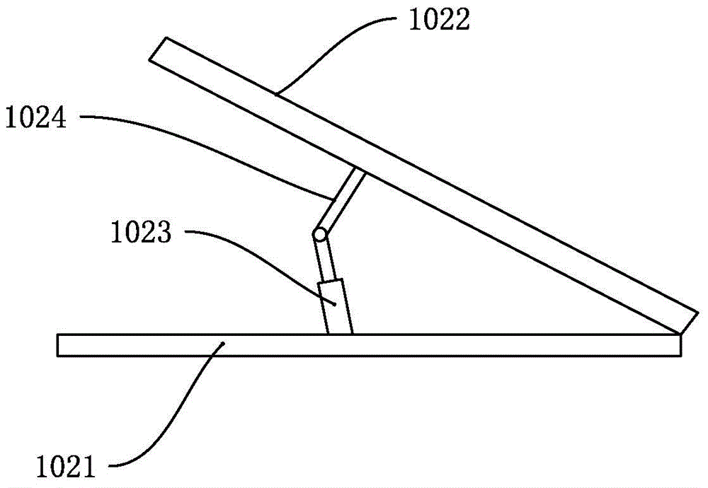
The invention discloses a semi-automatic alignment and exposure device of a printed circuit board (PCB). The semi-automatic alignment and exposure device comprises an alignment chamber and an exposure chamber, wherein an upper slipway and a lower slipway are respectively arranged in the alignment chamber and the exposure chamber and are in parallel, an upper alignment platform is arranged in the upper slipway and comprises a first working table, a first upper cover and an alignment mechanism, the first working table can slide along the upper slipway, the first upper cover is hinged with the first working table, a signal acquisition device is arranged above the first working table and can slide along the alignment chamber, the exposure chamber comprises an exposure device, the exposure device can do vertical movement along the exposure chamber, a lower alignment platform comprises a second working table, a second upper cover and an alignment mechanism, the second working table can slide along the lower slipway, the second upper cover is hinged with the second working table, the first working table and the second working table do movement relative to each other by a driving device, the semi-automatic alignment and exposure device also comprises a control system, and the control system controls opening and closing of a partition plate, controls the first working table and the second working table to do movement relative to each other and controls the alignment mechanism to automatically align. The semi-automatic alignment and exposure device has the advantages of positioning accuracy and high positioning efficiency.
Description
technical field [0001] The invention relates to an exposure machine, in particular to a semi-automatic alignment and exposure device for PCB boards. Background technique [0002] The PCB board needs to be aligned before exposure. The existing alignment device is manually aligned. There are some differences in this alignment. For example, the alignment between the PCB board and the film is observed by human eyes during alignment. In this case, the alignment error is large, the alignment accuracy is not high, and the alignment efficiency is relatively low. At the same time, due to the inaccurate alignment, after the PCB board is exposed, the qualified rate of the PCB board is relatively low. Contents of the invention [0003] The purpose of the present invention is to solve the deficiencies of the prior art and provide a semi-automatic alignment and exposure device for PCB boards. [0004] Technical scheme of the present invention is: [0005] A semi-automatic alignment an...
Claims
Login to View More Application Information
Patent Timeline
 Patent Type & Authority Applications(China)
IPC IPC(8): G03F7/20G03F9/00
Inventor 张家豪
Owner 永天机械设备制造(深圳)有限公司


