MRAM-using solid state hard disk and physical address-using reading/writing method

A technology of solid-state hard disk and physical address, which is applied in the directions of memory address/allocation/relocation, energy-saving computing, and climate sustainability. Guaranteed read and write performance and reduced costs

Inactive Publication Date: 2016-06-01
SHANGHAI CIYU INFORMATION TECH
View PDF6 Cites 10 Cited by
  • Summary
  • Abstract
  • Description
  • Claims
  • Application Information

AI Technical Summary

Problems solved by technology

However, the introduction of the write cache creates a new problem: once a power failure occurs, the content in the DRAM cache that has not been written to the NAND will be lost, causing the system to lose data or even damage the en

Method used


Image

  • MRAM-using solid state hard disk and physical address-using reading/writing method
  • MRAM-using solid state hard disk and physical address-using reading/writing method
  • MRAM-using solid state hard disk and physical address-using reading/writing method

Examples


Example Embodiment

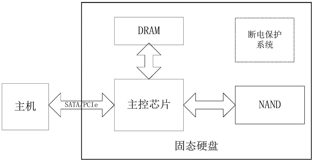
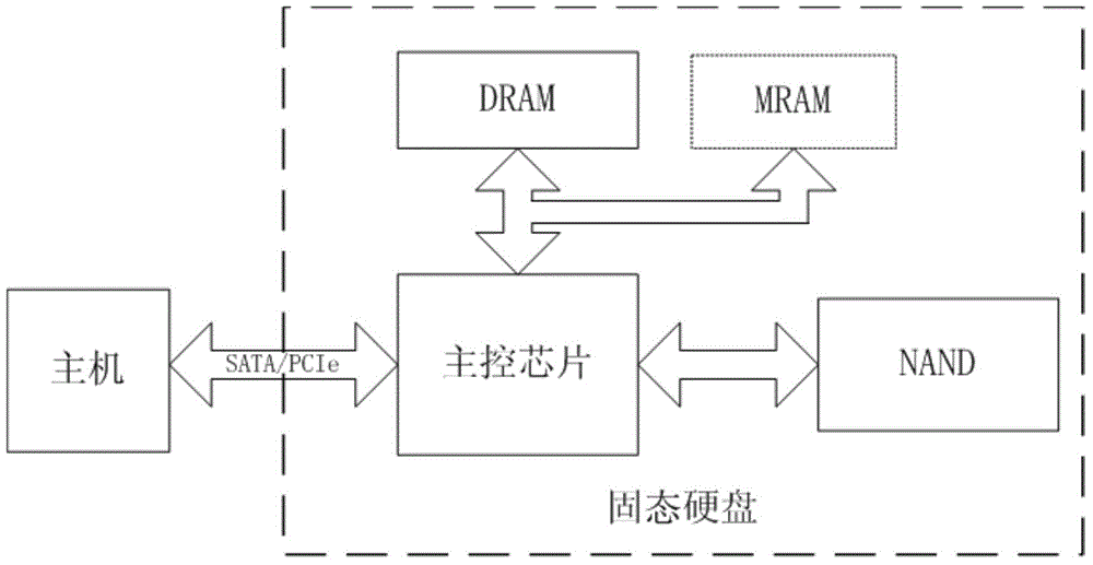
[0056] Such as Figure 4 As shown, the solid state drive of an embodiment of the present invention includes a main control chip and a set of NAND chips for storing data. The NAND chip is connected to the main control chip. The solid state drive further includes MRAM. The MRAM is connected to the main control chip. Including read and write cache.

[0057] The MRAM is connected to the main control chip of the solid-state hard disk through the DDRDRAM interface.

[0058] The NAND chip stores a logical address and a physical address comparison table. When the device is turned on, the file system reads from the NAND to the host memory. With this scheme, since the entire logical address and physical address comparison table is read into the host memory, the random read and write performance will not be sacrificed, but a large amount of memory in the host will be consumed, so this scheme is more suitable for servers.

[0059] The logical address and physical address comparison table is wri...


PUM


Abstract

The invention provides a solid state hard disk. The solid state hard disk comprises a main control chip, a group of NAND chips and an MRAM, wherein the NAND chips are used for storing data and are connected with the main control chip; the MRAM is connected with the main control chip; and the MRAM comprises a read/write cache. According to the solid state hard disk and a physical address-using reading/writing method provided by the invention, the MRAM comprises the read/write cache, so that the read/write performance can be ensured; a DDR DRAM is not used, and expensive and large-volume outage protection equipment is not needed, so that the cost and power consumption of the solid state hard disk are reduced; by using a host file system to process a logic address and physical address comparison list, the whole performance of the system is improved without loss; and the random read/write performance is not sacrificed and a lot of internal memory in the host is consumed, so that the scheme is more suitable for servers.

Description

technical field [0001] The invention relates to a solid-state hard disk, in particular to a solid-state hard disk using MRAM and a reading and writing method using physical addresses. Background technique [0002] Currently, the development of NAND flash memory technology has promoted the SSD industry. Such as figure 1 As shown, high-speed serial interfaces such as SATA, PICe and other technologies are used between the SSD and the host. The interior consists of a set of NAND chips used to store data, DDR DRAM (memory) used to support calculations and cache data, and a main control chip (SSD Controller). Sometimes a power failure protection system is also required. [0003] NAND is a storage device that reads and writes as a whole. The smallest readable unit is called a page, and the smallest erasable unit is called a block. A block is often composed of many pages. After the block is erased, the pages inside can be written separately Enter operation. Write operations are...

Claims


Application Information

Patent Timeline
IPC IPC(8): G06F12/02G06F12/08
CPCY02D10/00
Inventor 戴瑾
Owner SHANGHAI CIYU INFORMATION TECH
Why Eureka
Try Eureka