Latch and frequency divider
A technology of latches and transistors, applied in the direction of synchronous pulse counters, pulse technology, logic circuits, etc., can solve the problem of large power consumption, and achieve the effect of eliminating power consumption and reducing dynamic power consumption
- Summary
- Abstract
- Description
- Claims
- Application Information
AI Technical Summary
Problems solved by technology
Method used
Image

Examples
Embodiment Construction
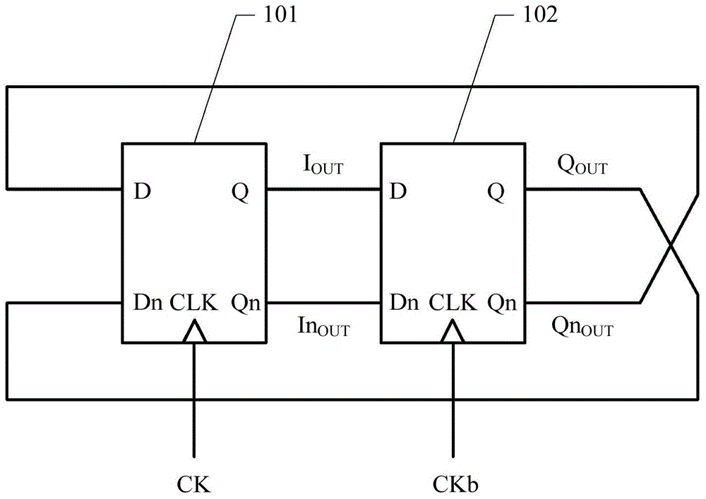
[0079] See figure 1 As shown, the high-speed frequency divider by two in the prior art may include latches 101 and 102, wherein the latches 101 and 102 are subsequent units of each other.
[0080] The frequency of the output signal of the high-speed frequency divider is 1 / 2 of the frequency of the input signal, and it can realize the output of the quadrature frequency division signal with a duty ratio of 25% or 75%.
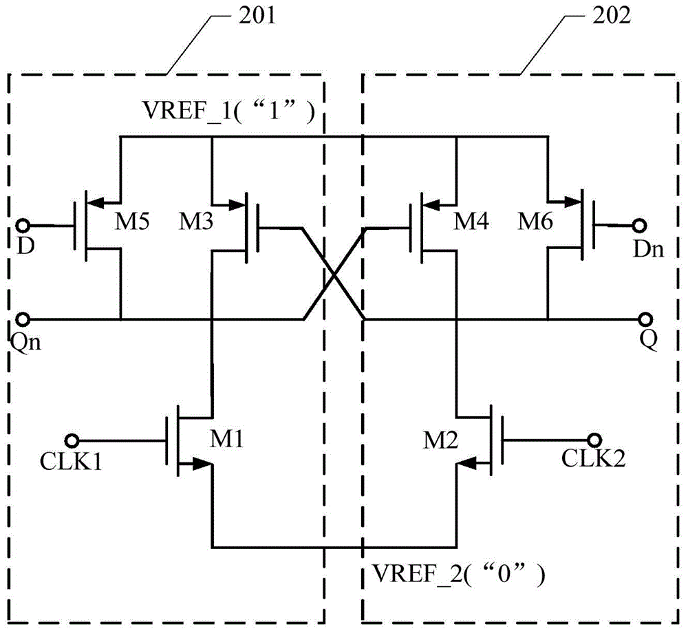
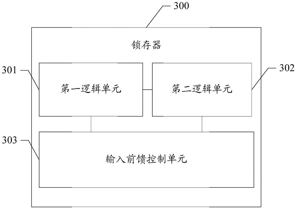
[0081] figure 2 A schematic circuit structure diagram of a latch in a high-speed frequency divider by two for realizing a frequency-divided signal with a duty cycle of 75% is shown. See figure 2 shown. The latch 200 includes a first logic unit 201 and a second logic unit 202 coupled between a power supply and a ground.
[0082] The first logic unit 201 has a first control terminal CLK1, a first signal input terminal D and a first signal output terminal Qn, and the second logic unit has a second control terminal CLK2, a second signal input terminal Dn and a ...
PUM
 Abstract
Description
Claims
Application Information