Organic light emission display panel

A light-emitting display, organic technology, used in diodes, semiconductor devices, electrical components, etc., can solve the problems of high production cost, low yield, complex film structure, etc., to achieve thinning, cost saving, and reduction of film structure. Effect

Inactive Publication Date: 2016-06-08
SHANGHAI TIANMA MICRO ELECTRONICS CO LTD +1
View PDF5 Cites 15 Cited by
  • Summary
  • Abstract
  • Description
  • Claims
  • Application Information

AI Technical Summary

Problems solved by technology

[0004] The organic light-emitting display panel provided by the prior art has complex film structure, high production cost and low yield

Method used


Image

  • Organic light emission display panel
  • Organic light emission display panel
  • Organic light emission display panel

Examples


Embodiment Construction

[0019] In order to make the above objects, features and advantages of the present invention more comprehensible, the present invention will be further described below in conjunction with the accompanying drawings and embodiments.

[0020] It should be noted that in the following description, specific details are set forth in order to fully understand the present invention. However, the present invention can be implemented in many other ways than those described here, and those skilled in the art can make similar extensions without departing from the connotation of the present invention. Accordingly, the present invention is not limited to the specific embodiments disclosed below.

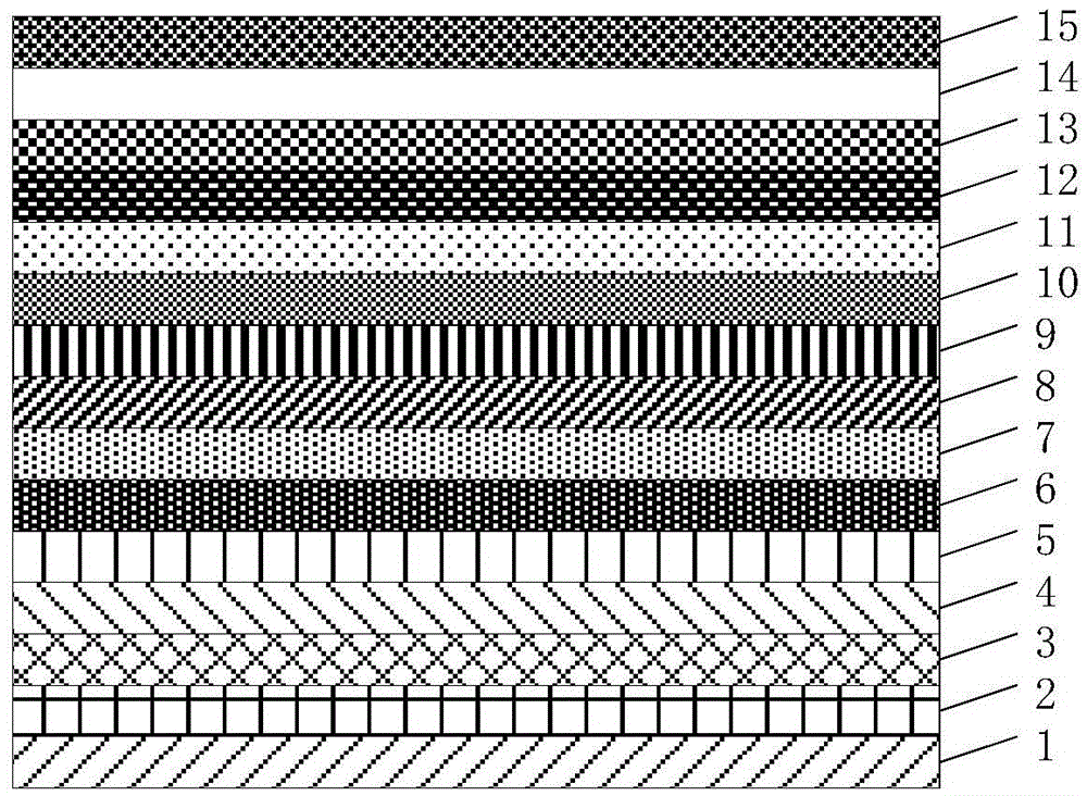
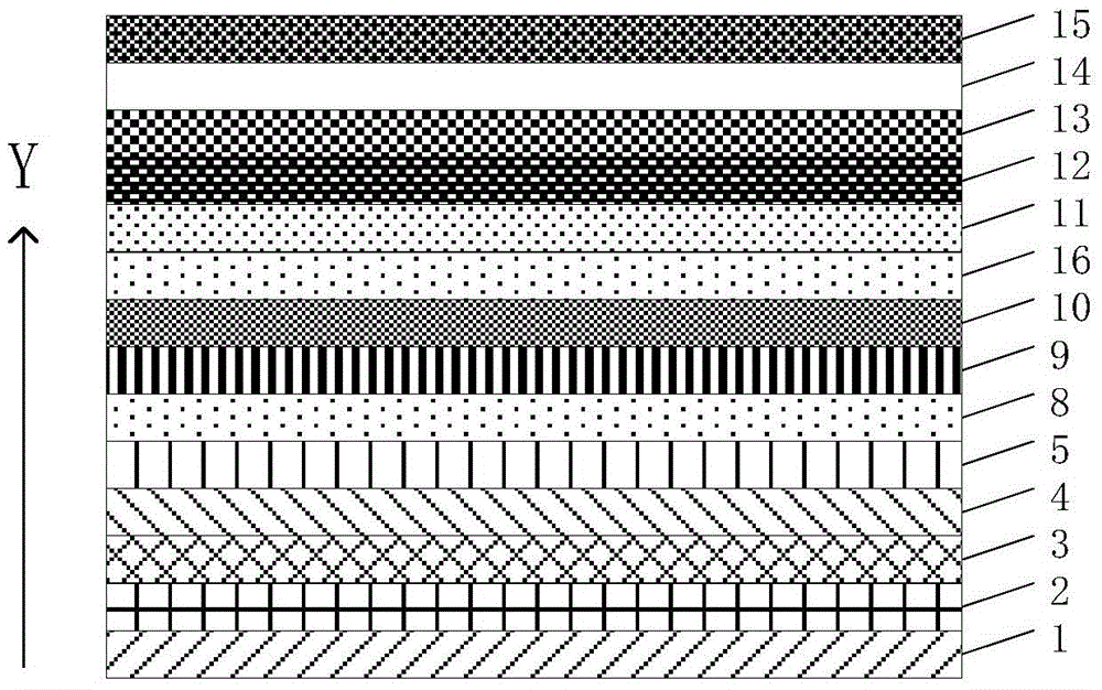
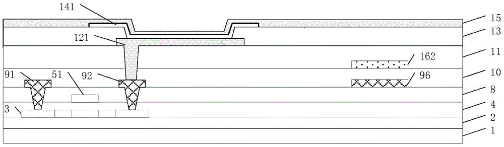
[0021] figure 2 It is a schematic diagram of the film layer structure of an organic light emitting display panel provided by an embodiment of the present invention. Please refer to figure 2 , the organic light-emitting display panel provided by the present invention includes a substrate 1, the ...


PUM


Abstract

The invention discloses an organic light emission display panel. The organic light emission display panel comprises a substrate, a source and drain metal layer, a passivation layer and a planarization layer, wherein the source and drain metal layer, the passivation layer and the planarization layer are formed on the substrate in sequence. The organic light emission display panel is characterized in that a conducting layer is arranged between the passivation layer and the planarization layer in a clamped mode. According to the organic light emission display panel, a film layer structure is omitted, so that the technological process is simplified, cost is reduced, and a displayer is light and thin.

Description

technical field [0001] The invention relates to the field of display technology, in particular to an organic light emitting display panel. Background technique [0002] The organic light-emitting display panel uses an organic light-emitting diode (Organic Light-Emitting Diode, OLED) as a light-emitting element, which has the advantages of self-illumination, high contrast, ultra-wide viewing angle, and low power consumption. [0003] figure 1 A film layer structure diagram of an organic light-emitting display panel provided in the prior art, including a substrate 1, and a buffer layer 2, a semiconductor film layer 3, a gate insulating film 4, a gate metal layer 5, and an insulating film formed on the substrate in sequence. layer 6, metal layer 7, interlayer insulating layer 8, source and drain metal layer 9, passivation layer 10, planarization layer 11, anode electrode layer 12, pixel definition layer 13, organic light emitting layer 14 and cathode electrode layer 15. [00...

Claims


Application Information

Patent Timeline
Patent Type & Authority Applications(China)
IPC IPC(8): H01L27/32H01L51/52
CPCH10K59/65H10K50/805
Inventor 姜文鑫
Owner SHANGHAI TIANMA MICRO ELECTRONICS CO LTD
Why Eureka
Try Eureka