Conductive film structure used for smart film
A technology of light-adjusting film and conductive film, which is applied in the direction of conductive layer, optics, nonlinear optics, etc. Poor rate and other issues
- Summary
- Abstract
- Description
- Claims
- Application Information
AI Technical Summary
Problems solved by technology
Method used
Image
Examples
Embodiment Construction
[0043] The descriptions of the following examples are only for illustrating the present invention, and are not intended to limit the aspect of the present invention. In the following embodiments and drawings, components that are not directly related to the present invention have been omitted and not shown, and the dimensional relationship between the components shown in the drawings is only for understanding, not for limitation. Actual implementation ratio.
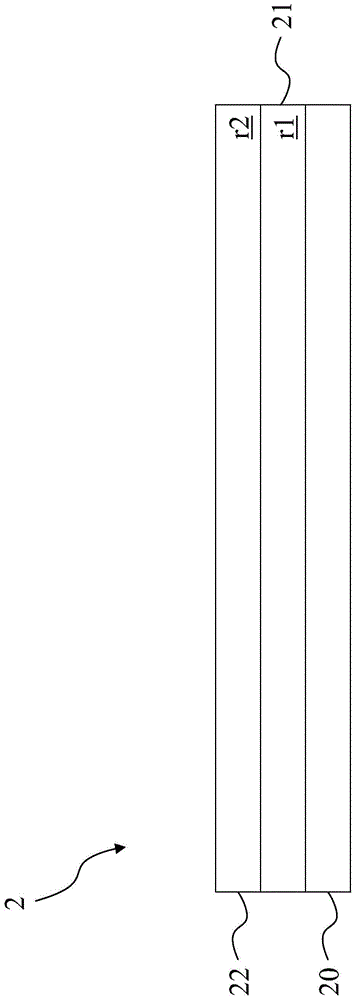
[0044] First, please refer to figure 2 , which is a cross-sectional view of a conductive film structure 2 for dimming films according to the first embodiment of the present invention. The conductive film structure 2 includes a base film layer 20 , a first transparent conductive film layer 21 and a second transparent conductive film layer 22 . Wherein, the first light-transmitting conductive film layer 21 is disposed on the base film layer 20 for reducing the resistance value and has a first light refraction index r1. ...
PUM
| Property | Measurement | Unit |
|---|---|---|
| thickness | aaaaa | aaaaa |
| thickness | aaaaa | aaaaa |
| thickness | aaaaa | aaaaa |
Abstract
Description
Claims
Application Information


