Thin film magnetic head and manufacturing method thereof

a thin film, magnetic head technology, applied in the direction of heads with metal sheet cores, instruments, nanoinformatics, etc., can solve the problems of increasing the electric resistance of the coil, increasing the temperature of the heat generation during a write operation, and reducing the number of coil turns to shorten the yoke length yl has a limit, so as to reduce the quantity of generated heat and reduce the resistance value of the coil

Active Publication Date: 2005-03-31
SAE MAGNETICS (HK) LTD +1
View PDF3 Cites 19 Cited by
  • Summary
  • Abstract
  • Description
  • Claims
  • Application Information

AI Technical Summary

Benefits of technology

[0013] An object of the present invention is to provide a thin film magnetic head and a magnetic recording device in which a coil resistance value is lowered and the quantity of generated heat is reduced as keeping the number of coil turns.

Problems solved by technology

However, since the number of turns of a coil is determined by a magneto motive force required, reducing the number of coil turns to shorten the yoke length YL has a limit.
On the other hand, in case of reducing the width of a coil without decreasing the number of turns, the electric resistance of the coil increases, so a temperature rise due to heat generation increases during a write operation.
If it is impossible to avoid a thermal protrusion, the floating height of a thin film magnetic head must be increased after all, which makes it impossible to meet a demand for a low floating height for a high recording density.
However, since this prior art discloses a structure in which the upper surfaces of the first conductors are covered with an insulating film, the sectional areas of the first conductors decrease by presence of the insulating film.
In short, the above-mentioned prior art does not disclose a technique of maximizing the sectional areas of the first conductors.
And the above-mentioned prior art fails to disclose the relation of conductors relative to a pole portion and a back gap.
Further, it is not necessarily preferable that the space between a conductor and each of a pole portion and a back gap is simply made narrow.
The reason is that when the space between a conductor and each of a pole portion and a back gap is made narrow, there is a risk that the space which has not completely been filled up may make a keyhole.
This prior art fails to disclose a means of solving the above-mentioned problem as well.

Method used


Image

  • Thin film magnetic head and manufacturing method thereof
  • Thin film magnetic head and manufacturing method thereof
  • Thin film magnetic head and manufacturing method thereof

Examples


embodiment 1

[0182] (1) Embodiment 1

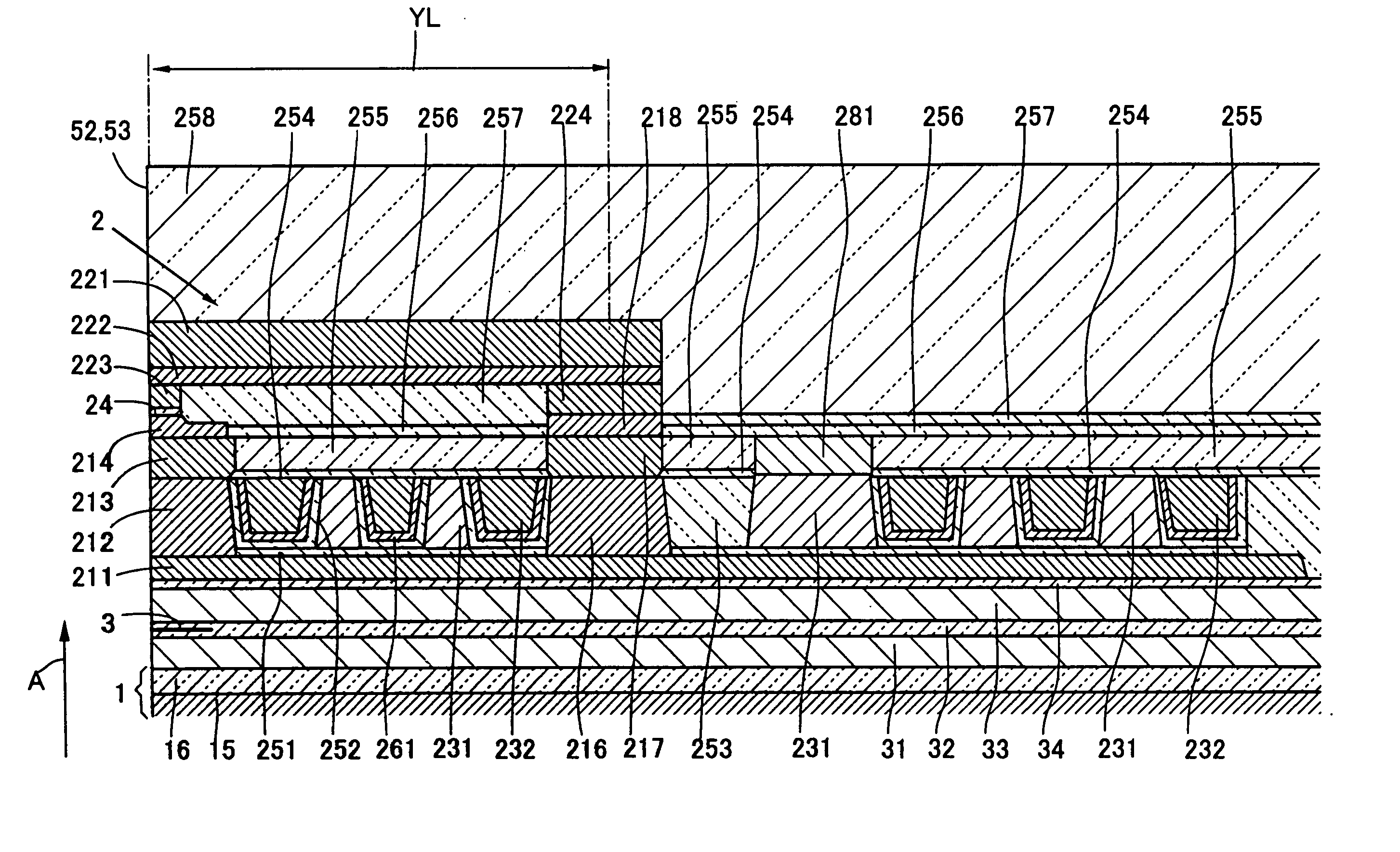
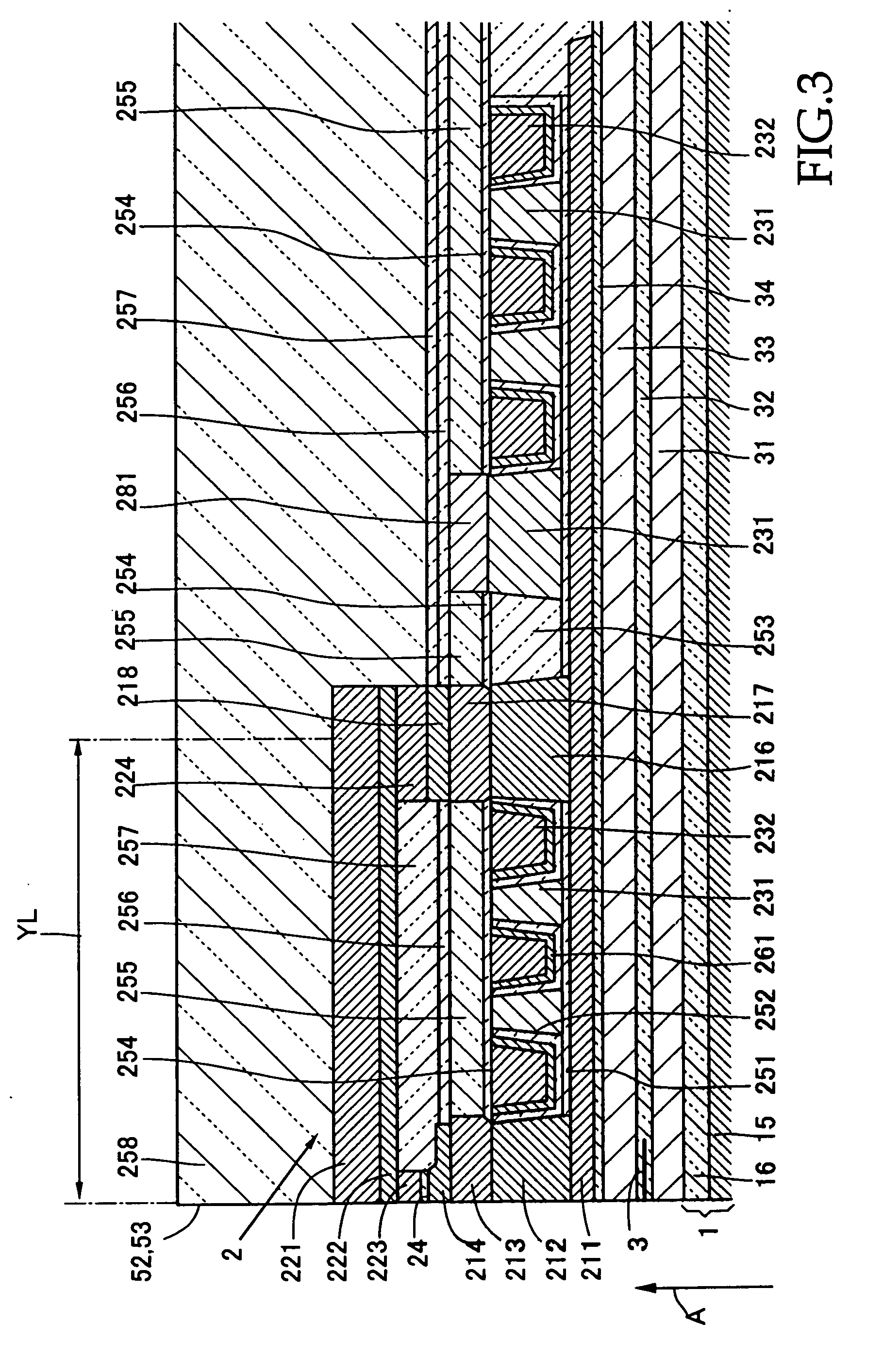
[0183] Embodiment 1 related to a manufacturing method is a process for manufacturing a thin film magnetic head of the first aspect having the first coil 231 and the second coil 232 (FIGS. 1 to 6). It is notified in advance that processes illustrated in FIGS. 11 to 44 are performed on a wafer.

[0184] First, referring to FIG. 11, on an insulating film 16 deposited on a base body 15 there are formed a first shield film 31, a read element 3, an insulating film 32, a second shield film 33, an insulating film 34 and a first magnetic film 211 by means of publicly known processes. After that, an insulating film 251 is formed on the flat surface of the first magnetic film 211, the insulating film 251 having an area slightly larger than an area necessary for forming a coil. On the surface of the insulating film 251 there is formed a seed film 260. The seed film 260 is formed so as to cover the surface of the insulating film 251 and the surface of the first magnetic film...

embodiment 2

[0215] (2) Embodiment 2

[0216] Embodiment 2 relates to a method for manufacturing a thin film magnetic head shown in FIGS. 7 and 8. FIGS. 45 to 68 show a process of manufacturing the same. It is notified in advance that processes illustrated in FIGS. 45 to 66 are also performed on a wafer.

[0217] First, referring to FIG. 45, a first shield film 31, a read element 3, an insulating film 32, a second shield film 33, an insulating film 34 and a first magnetic film 211 are formed on an insulating film 16 deposited to a base body 15 by means of publicly known processes. After that, an insulating film 251 having an area slightly larger than an area necessary for forming a coil is formed on the flat surface of the first magnetic film 211, and a seed film 260 is formed on the insulating film 251. The seed film 260 is formed so as to cover the surface of the insulating film 251 and the surface of the first magnetic film 211. The seed film 260 is made of a material suitable for a Cu-plating gro...

embodiment 3

[0240] (3) Embodiment 3

[0241] Embodiment 3 is a process of manufacturing a thin film magnetic head shown in FIGS. 9 and 10, and is illustrated in FIGS. 68 to 78. Processes which have been illustrated and described in embodiment 1 or 2 and are used also in embodiment 3 are referred to the description of embodiment 1 or 2 and the illustrations of the processes may be omitted.

[0242] (A) Process Leading to a State of FIG. 68

[0243]FIG. 68 shows a state in which the manufacturing processes shown in FIGS. 45 to 52 have been performed. In the state of FIG. 68, a flat spiral pattern of the second coil 232 is obtained by CMP, insulated from the first coil 231 by the insulating film 252. And the surfaces of the pole piece 212, the back gap piece 216 and the insulating film 253 are polished so as to form the same plane as the surfaces of the first coil 231 and the second coil 232.

[0244] (B) Process Leading to a State of FIG. 69

[0245]FIG. 69 shows a state in which the third coil 233, the pole ...


PUM

PropertyMeasurementUnit
taper anglesaaaaaaaaaa
thicknessaaaaaaaaaa

Abstract

The invention is directed to improvement of a write element of a thin film magnetic head. In said write element, a first coil and a second coil are provided on a first insulating film formed on one surface of a first magnetic film and surround in a spiral form a back gap portion. One of the first coil and the second coil is fitted into the space between coil turns of the other, insulated from the coil turns of the other by a second insulating film, and the first and second coils are connected to each other so as to generate magnetic flux in the same direction. One of said first coil and said second coil has a side surface being adjacent to the pole portion with the second insulating film and another side surface being adjacent to the back gap portion with the second insulating film, and each of said side surfaces has a taper angle making the sectional shape of the coil narrower in the lower part and wider in the upper part. The upper surfaces of said first and second coils form the same plane.

Description

BACKGROUND OF THE INVENTION [0001] 1. Field of the Invention [0002] The present invention relates to a thin film magnetic head, a magnetic recording apparatus using the same and a method for manufacturing the same, and particularly to improvement of a thin film magnetic head. [0003] 2. Discussion of Background [0004] In a write element provided inside a thin film magnetic head, a first pole portion and a second pole portion faces each other with a gap film between them at an air bearing surface (hereinafter, referred to as ABS) side (hereinafter, referred to as the front part), and a back gap is formed by joining a lower magnetic film connected to the first pole portion and an upper magnetic film connected to the second pole portion at the rear part opposite to the ABS. Around the back gap, a flat coil surrounding the back gap is positioned on a plane which is in parallel with the surfaces of the lower magnetic film and the upper magnetic film and nearly perpendicular to the ABS. Th...

Claims


Application Information

Patent Timeline
Patent Type & Authority Applications(United States)
IPC IPC(8): G11B5/147G11B5/17G11B5/31G11B5/39
CPCB82Y10/00B82Y25/00G11B5/17G11B5/3116G11B5/3163Y10T29/49062G11B5/3909G11B2005/3996Y10T29/4906Y10T29/49064G11B5/3906
Inventor SASAKI, YOSHITAKAKAMIGAMA, TAKEHIROITOH, HIROYUKI
Owner SAE MAGNETICS (HK) LTD
Why Eureka
Try Eureka