IC appearance inspection device
A technology of appearance inspection and qualified inspection, which is applied in the direction of sorting, optical testing for defects/defects, etc., can solve problems such as the inability to effectively improve production efficiency, increase sorting and classification, and single packaging methods, so as to improve production efficiency, reduce actions, and improve The effect of testing efficiency
- Summary
- Abstract
- Description
- Claims
- Application Information
AI Technical Summary
Problems solved by technology
Method used
Image

Examples
Embodiment Construction
[0029] The technical solution in the embodiment will be specifically, clearly and completely described below in conjunction with the drawings in the embodiment.
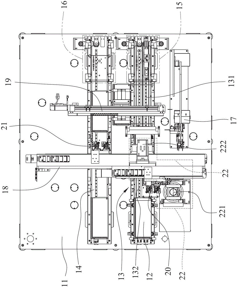
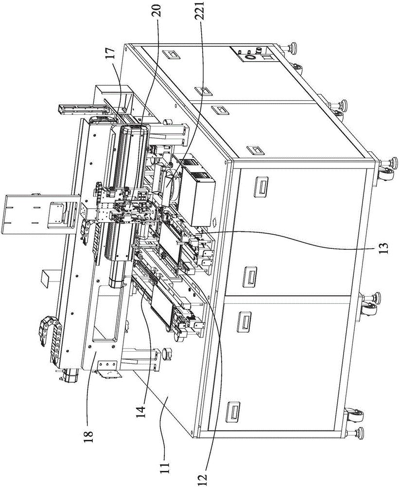
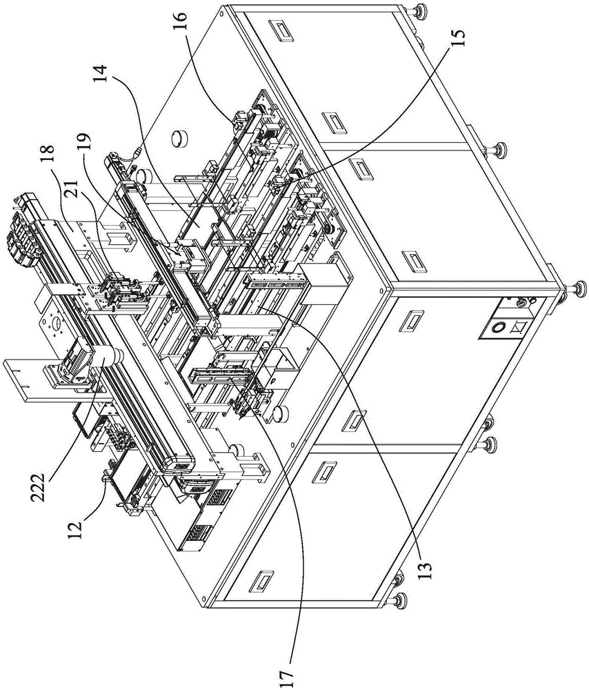
[0030] see figure 1 , 2 And shown in 3, the present invention provides a kind of IC appearance inspection device, comprise a machine platform 11, on the platform of machine platform 11, feed module 12, the first transfer track 13, the second transfer track 14, good product Stacking module 15, defective product stacking module 16, and material tube packaging module 17. In addition, a gantry 18 straddling the first transfer rail 13 and the second transfer rail 14 and a tray pick-and-place module 19 are installed on the machine platform 11 according to different configuration directions. Different side walls of the gantry 18 are respectively installed with movable The first pick-and-place module 20 and the second pick-and-place module 21 move along the frame body.
[0031] The feeding module 12 is a three-dimensional...
PUM
 Abstract
Description
Claims
Application Information
 - Generate Ideas
- Intellectual Property
- Life Sciences
- Materials
- Tech Scout
- Unparalleled Data Quality
- Higher Quality Content
- 60% Fewer Hallucinations
Browse by: Latest US Patents, China's latest patents, Technical Efficacy Thesaurus, Application Domain, Technology Topic, Popular Technical Reports.
© 2025 PatSnap. All rights reserved.Legal|Privacy policy|Modern Slavery Act Transparency Statement|Sitemap|About US| Contact US: help@patsnap.com