A non-destructive positioning method of goi failure point and goi failure analysis method

A locating method and failure point technology, applied in the direction of analyzing materials, using wave/particle radiation for material analysis, measuring devices, etc., can solve the problems of GOI failure point damage, time-consuming, etc., to reduce production time, improve accuracy and success. The effect of high-speed, high-precision positioning

CN105699410BActive Publication Date: 2018-05-29WUHAN XINXIN SEMICON MFG CO LTD
7 Cites 0 Cited by

Patent Information

Authority / Receiving Office
CN · China
Patent Type
Patents(China)
Current Assignee / Owner
Publication Date
2018-05-29

Smart Images

  • Figure 1
    Figure 1
Patent Text Reader

Abstract

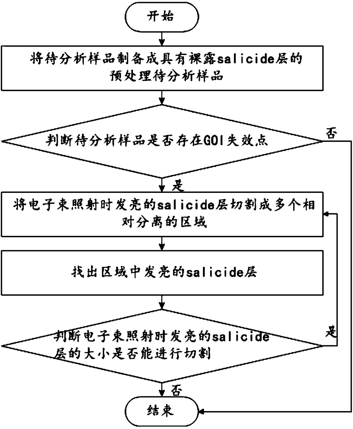
The invention relates to a non-destructive positioning method of a GOI failure point and a GOI failure analysis method, comprising step 1, removing the metal interconnection layer of the sample to be analyzed, and obtaining a pretreated sample to be analyzed with a bare salicide layer; step 2, based on the PVC method, Use an electron beam to irradiate the salicide layer of the pretreated sample to be analyzed, and observe whether it is shiny; if yes, then there is a GOI failure point in the sample to be analyzed, and perform step 3; if not, there is no GOI in the sample to be analyzed Failure point, end operation; step 3, cut the salicide layer that shines when electron beam is irradiated into multiple relatively separated areas; step 4, again based on PVC method, use electron beam to irradiate the area, and find out the area The shiny salicide layer in the medium; step 5, execute step 3 and step 4 in a loop until the size of the shiny salicide layer cannot be cut when the electron beam is irradiated, and then end the operation. The invention realizes high-precision positioning of the failure point of the GOI, and the whole positioning process will not cause further damage to the failure point of the GOI.
Need to check novelty before this filing date? Find Prior Art

Description

Technical field

[0001] The invention relates to the technical field of semiconductor manufacturing, in particular to a method for non-destructive positioning of GOI failure points and a GOI failure analysis method. Background technique

[0002] The GOI test is to test the withstand voltage of the gate oxide layer in the MOS device. If the GOI test fails, GOI failure analysis is required to find out the cause of the GOI test failure. The main process of traditional GOI failure analysis is: obtain an optical picture of the GOI failure point of the sample to be analyzed through hot spot analysis, compare the optical picture with the electron microscope picture of the sample to be analyzed, locate the GOI failure point, and then use FIB to prepare TEM Samples, TEM observation and elemental analysis are performed to obtain the composition of the abnormal substance at the GOI failure point. However, the GOI failure point location based on hot spot analysis will lead to further destruc...

Examples

Embodiment Construction

[0027] The principles and features of the present invention will be described below with reference to the accompanying drawings. The examples cited are only used to explain the present invention, and are not used to limit the scope of the present invention.

[0028] Such as figure 1 As shown, a GOI failure point lossless location method includes the following steps:

[0029] Step 1, removing the metal interconnection layer of the sample to be analyzed to obtain a preprocessed sample to be analyzed with a bare salicide layer; the metal interconnection layer of the sample to be analyzed is removed by mechanical grinding and / or chemical etching.

[0030] Step 2. Based on the PVC method, irradiate the salicide layer of the pre-analyzed sample with an electron beam and observe whether it is shiny; if yes, the sample to be analyzed has a GOI failure point, go to step 3; if not, then If there is no GOI failure point in the sample to be analyzed, the operation is ended.

[0031] Step 3, cutt...