
Method and device for self-adaptive adjustment of reading timing path by chip

An adaptive adjustment, chip technology, applied in the direction of electrical digital data processing, instruments, etc., can solve the problem of long data path and delay at the initiator of the SRAM return command, and achieve the effect of increasing the maximum operating frequency and shortening the timing path

Active Publication Date: 2018-09-28
FUZHOU ROCKCHIP SEMICON
View PDF5 Cites 0 Cited by
  • Summary
  • Abstract
  • Description
  • Claims
  • Application Information

AI Technical Summary

Problems solved by technology

At the same time, due to the complexity of the SRAM storage circuit, and in terms of function, it is required to complete the operation at the next clock beat when the command is received, so when the chip frequency increases rapidly, the reading speed of the SRAM obviously becomes the limit of the chip frequency. Critical Path
At present, the timing path of chip reading is from SRAM command collection to SRAM internal fetching and output to the SRAM port, then to the unit that issues the command, and then to the unit that issues the command to complete data sampling, especially when there are many modules mounted on the bus, SRAM The data path back to the originator of the command will be very long and cause a large delay

Method used


Image

  • Method and device for self-adaptive adjustment of reading timing path by chip
  • Method and device for self-adaptive adjustment of reading timing path by chip

Examples


Embodiment Construction

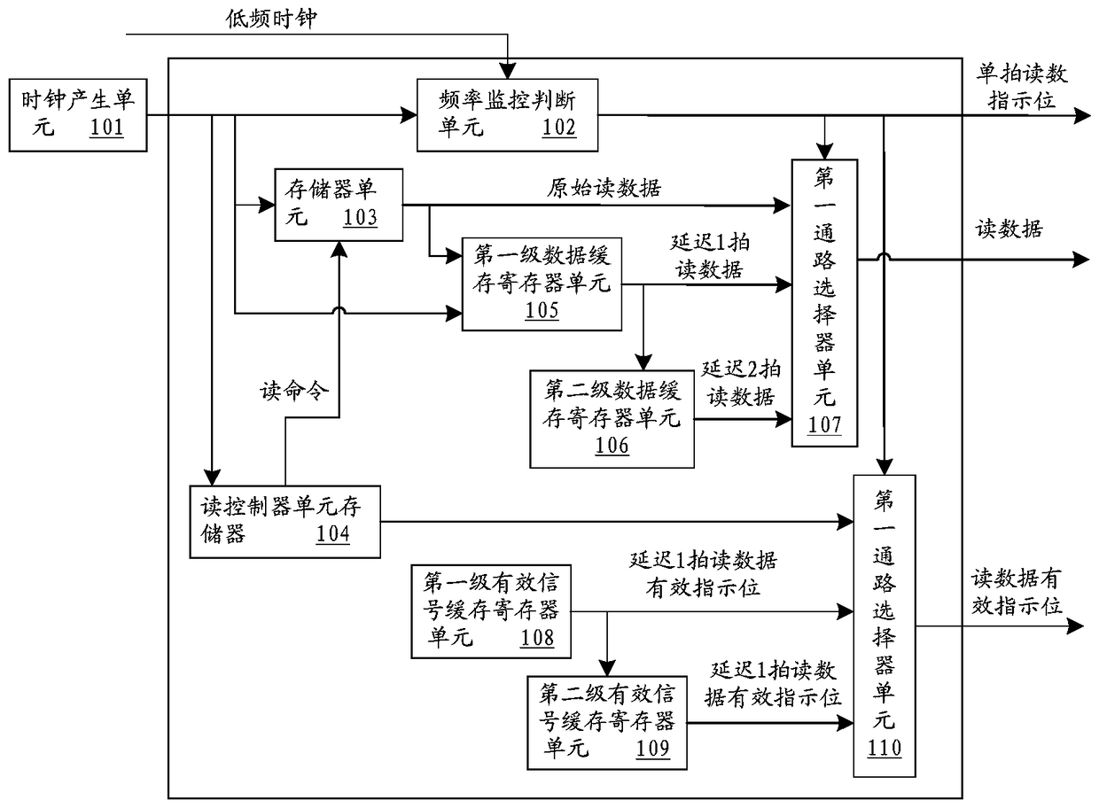
[0015] The method for self-adaptively adjusting the reading timing path of the chip of the present invention comprises the following steps:

[0016] After the chip initialization is completed, it starts to work and generates a working clock;

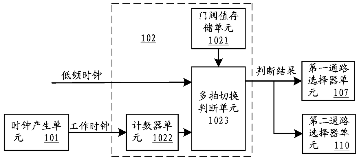
[0017] Judging the working clock frequency according to the low-frequency clock input by the chip and the working clock;

[0018] The read control unit memory outputs a read command to the memory unit to perform a read operation, and at the same time sets the valid indicator bit of the original read data to be valid after one cycle of the read command;

[0019] According to the received read command and the working clock, the memory unit outputs the original read data after the read command is sampled by the working clock, and after the delay time of the read action inherent in the circuit;

[0020] The original read data is respectively delayed by one cycle by one stage and two cycles by two stages to obtain read data delayed by one cy...


PUM


Abstract

The invention provides a method and a device for a chip to adaptively regulate a reading time sequence path. A read control unit memory outputs a read command to a memory unit to carry out a read operation, and meanwhile, the effective indication bit of the original read data is set to be effective after one period of the read command; according to the received read command and a work clock, the memory unit outputs the original read data; the original read data are individually delayed for one period and two periods; according to a judgment result of the frequency of the work clock, an access selection operation is carried out, one path of three inputs, including the original read data, the read data which is delayed for one period and the read data which is delayed for two periods, is selected as output read data; the effective indication bit of the original read data is individually delayed for one period and two periods; and according to the judgment result of the frequency of the work clock, the access selection operation is carried out, one path of three inputs, including the effective indication bit of the original read data and the effective indication bits of the two delayed read data, is selected as the effective indication bit of the output read data.

Description

technical field [0001] The invention relates to a method and a device for chip self-adaptive adjustment of the reading timing path. Background technique [0002] With the development of SOC chip technology, users have higher and higher requirements for chip performance. Since the operating frequency of the chip directly affects the performance, the main frequency of the chip is getting higher and higher. At the same time, due to the complexity of the SRAM storage circuit, and in terms of function, it is required to complete the operation at the next clock beat when the command is received, so when the chip frequency increases rapidly, the reading speed of the SRAM obviously becomes the limit of the chip frequency. Critical Path. At present, the timing path of chip reading is from SRAM command collection to SRAM internal fetching and output to the SRAM port, then to the unit that issues the command, and then to the unit that issues the command to complete data sampling, espe...

Claims


Application Information

Patent Timeline
Patent Type & Authority Patents(China)
IPC IPC(8): G06F13/16
CPCG06F13/161
Inventor 廖裕民江显舟
Owner FUZHOU ROCKCHIP SEMICON
Learn More