Peripheral compensation system of pixel matrix, method thereof and display system

A technology of pixel matrix and peripheral compensation, applied in static indicators, instruments, etc., can solve the problems of increased chip area, complex structure of digital-to-analog conversion modules, increased power consumption, etc.

Active Publication Date: 2016-06-22
PEKING UNIV SHENZHEN GRADUATE SCHOOL
View PDF4 Cites 49 Cited by
  • Summary
  • Abstract
  • Description
  • Claims
  • Application Information

AI Technical Summary

Problems solved by technology

The disadvantage of this method is that the number of bits of the added signal will be large, so the structure of the digital-to-analog conversion module will be very complicated; if the original signal and the compensated signal are added in the analog domain, a high-voltage adder may be required, not only It will increase the chip area and increase the power consumption

Method used


Image

  • Peripheral compensation system of pixel matrix, method thereof and display system
  • Peripheral compensation system of pixel matrix, method thereof and display system
  • Peripheral compensation system of pixel matrix, method thereof and display system

Examples


Embodiment 1

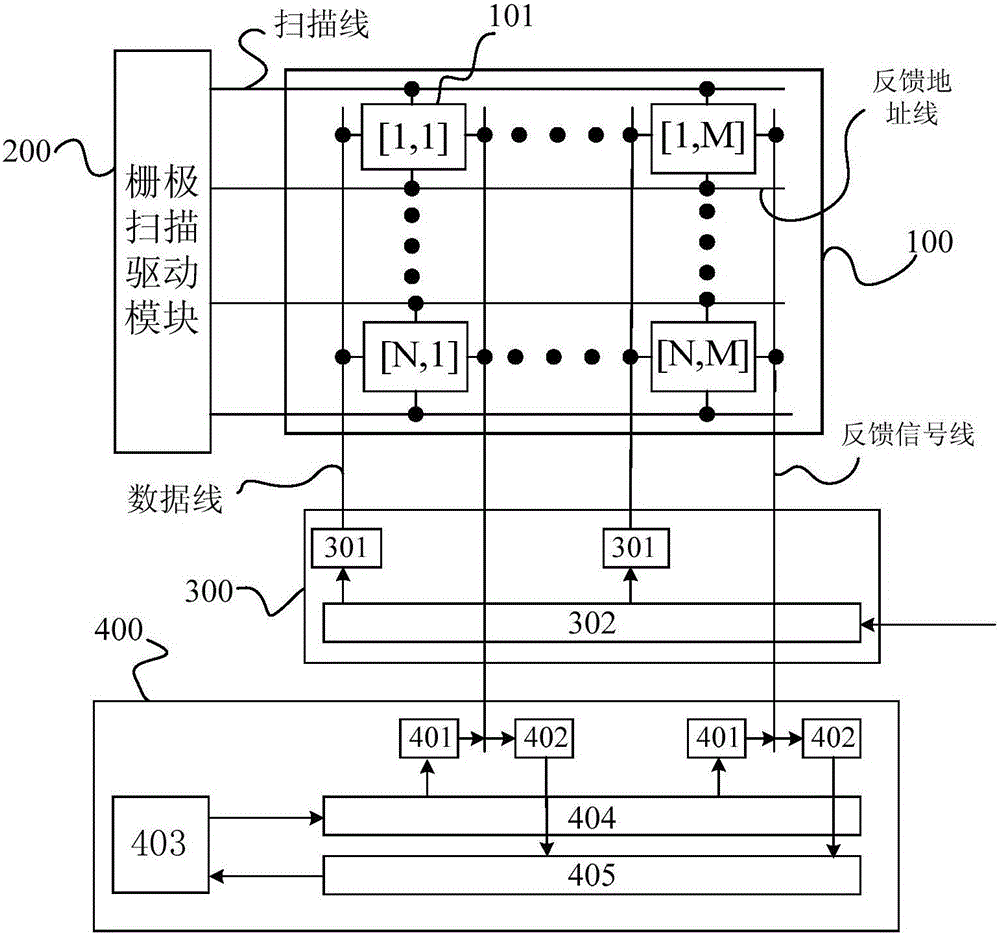
[0046]Please refer to figure 2 , this embodiment discloses a display system, which includes a pixel matrix 100, and a peripheral compensation system of the pixel matrix (hereinafter referred to as the peripheral compensation system).

[0047] The pixel matrix 100 includes N rows and M columns of pixel units 101, N rows of scanning lines and M columns of data lines. The pixel units 101 are connected to respective scanning lines and data lines, and both N and M are positive integers.

[0048] The peripheral compensation system includes a gate scan driving module 200 , a column data driving module 300 and a compensation module 400 , which will be described in detail below.

[0049] The gate scanning driving module 200 is used to send scanning signals to the pixel matrix 100 through scanning lines to sequentially gate each row of pixel units 101 in one frame; The pixel units 101 are connected to send a detection control signal to the pixel matrix 100 through a feedback address l...

Embodiment 2

[0078] This embodiment discloses a method for a peripheral compensation system of a pixel matrix. In one embodiment, it can be implemented by the display system and the peripheral compensation system disclosed in Embodiment 1. Specific instructions are given below.

[0079] The method disclosed in this embodiment includes a light-emitting operation frame and a detection compensation frame.

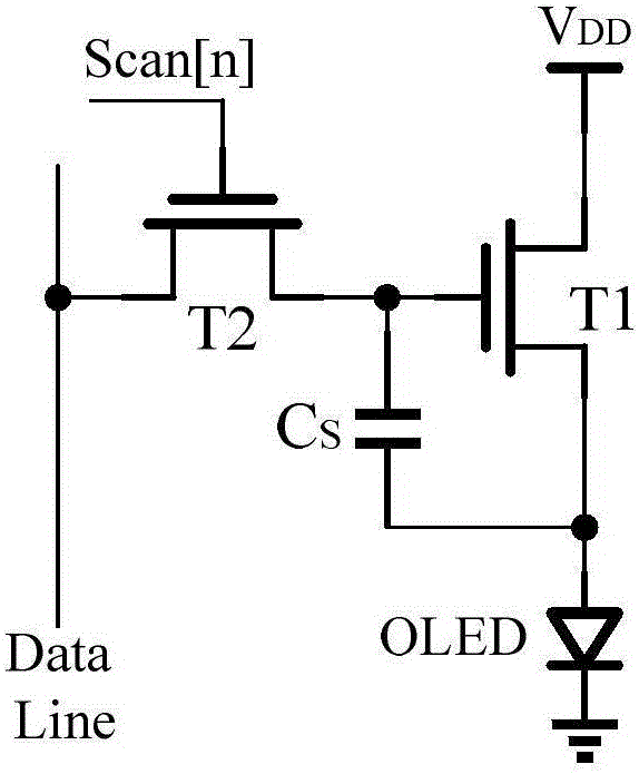
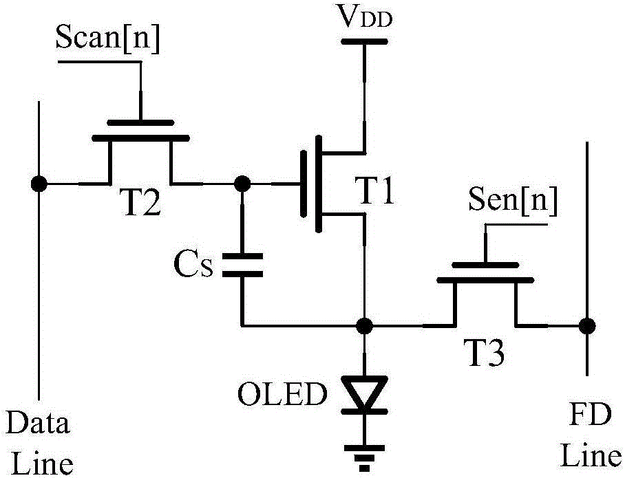
[0080] In the light-emitting operation frame, the operation on the pixel unit 101 is also performed row by row, which includes (1) data writing operation and (2) light-emitting operation. Specifically, (1) data writing operation: in a light-emitting operation frame of one frame, any pixel unit 101 in the nth row at t n Within a time period, where 1≤n≤N, the gate scanning driving module 200 enables the scanning line Scan[n] and the feedback address line Sen[n] of the pixel unit 101 in this row to be valid, and the column data driving module 300 and the compensation module 400 respectively ...

Embodiment 3

[0110] This embodiment discloses a method for a peripheral compensation system of a pixel matrix. In one embodiment, it can be implemented by the display system and the peripheral compensation system disclosed in Embodiment 1. Specific instructions below

[0111] One difference from Embodiment 2 is that the operation of the light-emitting operation frame in Embodiment 2 is performed when the display system is turned on and / or turned off, but this embodiment does not need to write into the black matrix.

[0112] The method disclosed in this embodiment also includes a lighting operation frame and a detection compensation frame.

[0113] The operation of the light-emitting operation frame is the same as that in the second embodiment, and will not be repeated here.

[0114] In a detection and compensation frame of one frame, each row of pixel units (101) performs the following operations in sequence: (1) writing of reference voltage: when it is the turn of a specific row of pixel...


PUM


Abstract

The invention discloses a peripheral compensation system of a pixel matrix, a method thereof and a display system. The peripheral compensation system comprises a grid scan driving module 200, a column data driving module 300 and a compensation module 400. The compensation module 400 is respectively connected with M columns of pixel units 101 via M columns of feedback signal lines and is used for detecting the variation of the electrical characteristics of a pixel matrix 100 so as to send a second display signal to the pixel matrix 100 and compensate each of the pixel units 101. According to the technical scheme of the invention, the addition of first display signals and second display signals in the pixel units is realized, so that accurate gamma correction of first display signals is realized at the same time. Meanwhile, the structure is simple. A first digital-to-analog conversion module and a second digital-to-analog conversion module are also low in the number of bits. On the condition that the addition mode of analog domains is conducted, an original high-voltage analog adder can be converted to a medium-voltage adder or a low-voltage adder.

Description

technical field [0001] The present application relates to the technical field of displays, in particular to a peripheral compensation system for a pixel matrix, a method thereof, and a display system. Background technique [0002] Active matrix organic light-emitting diode (Active Matrix Organic Light-Emitting Diode, OLED) has been widely studied in recent years due to its advantages of high brightness, high luminous efficiency, wide viewing angle and low power consumption, and has been rapidly applied to a new generation of display systems. . The traditional AMOLED pixel unit is a structure of two thin film field effect transistors (ThinFilmTransistor, TFT) and a storage capacitor, such as figure 1 As shown, where T1 is the driving transistor, T2 is the switching transistor, C S For storage capacitors and OLEDs for light emitting devices. The switching transistor T2 responds to the signal from the scan control signal line, samples the signal from the data line, and the s...

Claims


Application Information

Patent Timeline
Patent Type & Authority Applications(China)
IPC IPC(8): G09G3/3225
CPCG09G3/3225
Inventor 张盛东王翠翠林兴武
Owner PEKING UNIV SHENZHEN GRADUATE SCHOOL
Why Eureka
Try Eureka