User register state capture circuit adopting single-event hardened FPGA (field programmable gate array)

A single-particle reinforcement and register technology, applied in static memory, digital memory information, instruments, etc., can solve problems such as short circuit or open circuit of interconnection lines, inability to know the user's logic state, and partial circuit function errors, achieving wide applicability, reducing The effect of the cumulative effect of single-event flipping

Active Publication Date: 2016-06-22
BEIJING MXTRONICS CORP +1
View PDF5 Cites 7 Cited by
  • Summary
  • Abstract
  • Description
  • Claims
  • Application Information

AI Technical Summary

Problems solved by technology

[0004] When the FPGA chip is used in the space radiation environment, the space high-energy particles passing through the FPGA will cause an instantaneous current on the circuit node, causing the configuration storage unit SRAM in the configuration memory array to undergo a single-event flip, and the circuit in some areas will produce local functional errors. , short circuit or open circuit of the interconnection wire, making the circuit in this area unable to work normally
[0005] At present, it is possible to judge whether the configuration memory array in the FPGA chip has a single-event flip by reading back the configuration m

Method used


Image

  • User register state capture circuit adopting single-event hardened FPGA (field programmable gate array)
  • User register state capture circuit adopting single-event hardened FPGA (field programmable gate array)
  • User register state capture circuit adopting single-event hardened FPGA (field programmable gate array)

Examples


Embodiment Construction

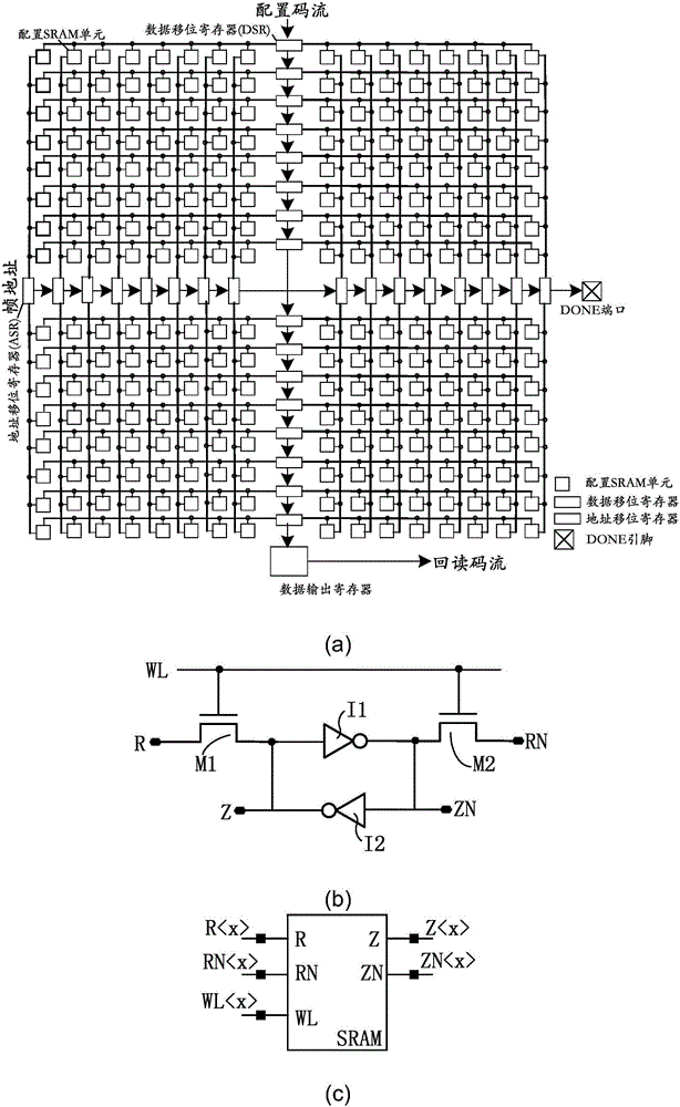
[0031] The SRAM FPGA chip completes the configuration by loading the specified configuration data into the internal configuration memory array (CSRAM), which contains a large number of SRAM storage cells. Such as figure 2 (b) shows the SRAM memory cell circuit, which includes two inverters I1, I2 and two transistors M1 and M2. The output of each inverter is connected to the input of the other inverter to form an interlock Structure, the source terminal of the transistor M1 is connected to the configuration data input signal R, the drain terminal is connected to the input terminal of the inverter I1, the gate terminal is controlled by the address decoding signal WL, and the source terminal of the transistor M2 is opposite to the configuration data input signal R The phase signal RN is connected, the drain terminal is connected to the input terminal of the inverter I2, the gate terminal is controlled by the address decoding signal WL, the output terminal of the inverter I2 is Z, ...


PUM


Abstract

A user register state capture circuit adopting a single-event hardened FPGA (field programmable gate array) comprises a user register, a transistor M3, a transistor M4, an SRAM (static random-access memory) storage unit and a capture signal generation circuit, wherein the transistor M3 and the transistor M4 are arranged between the user register and the SRAM storage unit; the capture signal generation circuit generates an output signal CAPTURE, controls conduction of the transistor M3 and the transistor M4 and realizes data capture readback. Compared with the prior art, the state capture circuit has the advantages that through capture readback operation, dynamic partial reconfiguration can be performed if the condition that configuration bit stream stored in the CSRAM (custom SRAM) has single-event upset is discovered, corresponding logic can be reset if the state of the SRAM storage unit for storing the captured user register state in the CSRAM has an error, so that the single-event upset accumulation effect of an FPGA chip is reduced remarkably.

Description

Technical field [0001] The invention relates to a technology for capturing values ​​in a user register, in particular to a single-event reinforced FPGA user register state capturing circuit. Background technique [0002] Such as figure 1 Shown is the structure of the field programmable gate array FPGA. The input and output ports (IOB) are located around the chip, the configurable logic module (CLB) is arranged in an array inside, and the block memory (BRAM) is interspersed in the configurable logic module (CLB). In ), FPGA also includes configuration logic, configuration interface and other components, such as programmable interconnect structure and configuration memory array (CSRAM) spreading over the entire FPGA chip, connecting various modules. [0003] The SRAM FPGA chip does not have any logic function before configuration. It completes the function configuration by loading the configuration data specified by the user application into the internal configuration memory array (C...

Claims


Application Information

Patent Timeline
IPC IPC(8): G11C19/28G11C19/38
CPCG11C19/28G11C19/38
Inventor 林彦君陈雷张彦龙张帆刘增荣赵元富王硕方新嘉
Owner BEIJING MXTRONICS CORP
Why Eureka
Try Eureka