A manufacturing method for a groove type super junction

A manufacturing method and super junction technology, applied in semiconductor/solid-state device manufacturing, electrical components, circuits, etc., can solve problems such as poor reverse breakdown voltage uniformity, and achieve the effect of improving in-plane uniformity

Active Publication Date: 2016-06-22
SHANGHAI HUAHONG GRACE SEMICON MFG CORP
View PDF6 Cites 5 Cited by
  • Summary
  • Abstract
  • Description
  • Claims
  • Application Information

AI Technical Summary

Problems solved by technology

In the etching of trenches, the morphology of trenches in different regions of the same semiconductor substrate wafer is not completely the same, and the reverse breakdown voltage of super junction devices is greatly affected by the morphology of trenches, making Poor uniformity of reverse breakdown voltage of superjunction devices on the same wafer

Method used


Image

  • A manufacturing method for a groove type super junction
  • A manufacturing method for a groove type super junction
  • A manufacturing method for a groove type super junction

Examples


Embodiment Construction

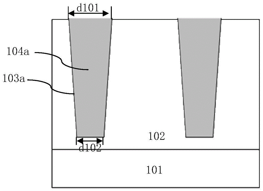
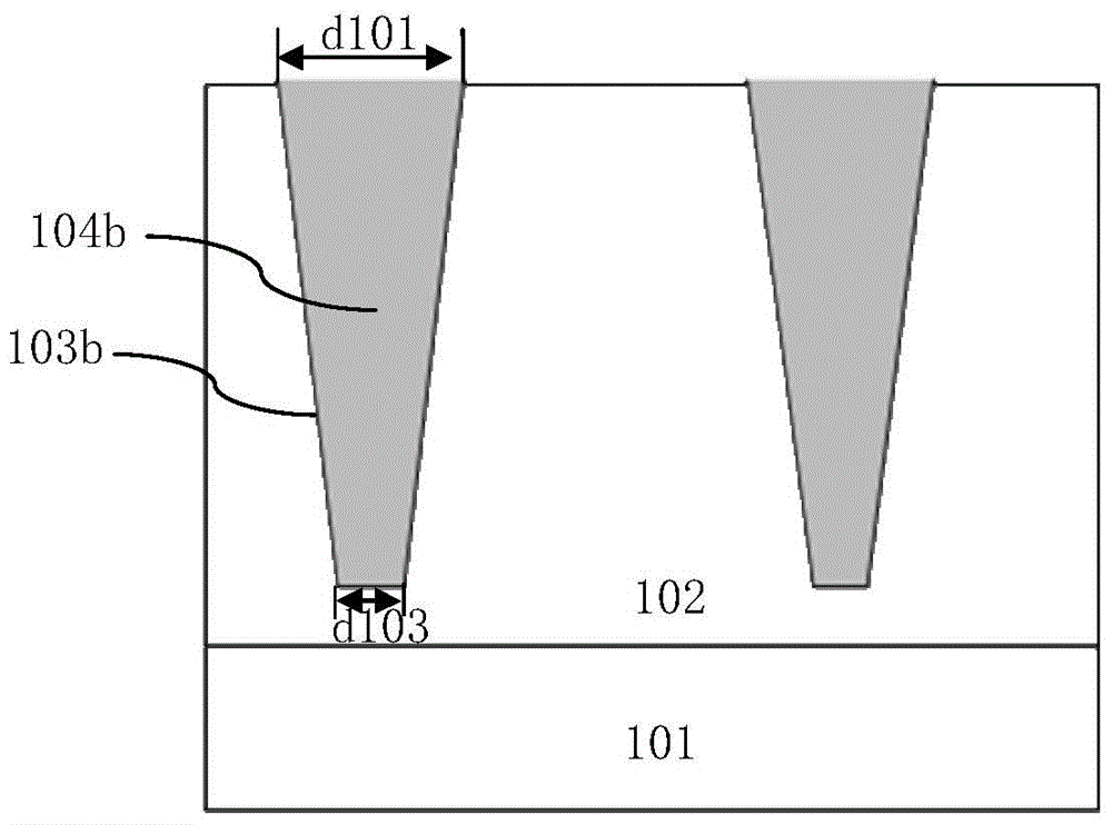
[0032] Such as Figure 1A As shown, it is a schematic diagram of the structure of a super junction located in the edge region of the wafer formed by the existing trench-type super junction manufacturing method; as Figure 1B Shown is a schematic diagram of the structure of the super junction located in the middle region of the wafer formed by the existing trench-type super junction manufacturing method; the existing trench-type super junction manufacturing method includes the following steps:

[0033] Step 1. Provide a semiconductor substrate wafer 101, on the surface of the semiconductor substrate wafer 101, a first conductivity type epitaxial layer 102 is formed, and the N-type epitaxial layer 102 is taken as an example for illustration below;

[0034] Step 2, using a photolithography process to define a trench formation area and open the trench formation area; in the existing method, the size of the trenches at different positions on the semiconductor substrate wafer 101 is ...


PUM

PropertyMeasurementUnit
Thicknessaaaaaaaaaa

Abstract

The invention discloses a manufacturing method for a groove type super junction. The method comprise the following steps: 1, a wafer, on which a first conductive type epitaxial layer forms, is provided; 2, a groove formation area is defined through adoption of a photoetching process, and the top width of the groove positioned at the middle area of the wafer is made to be larger than the top width of each groove at the edge area; 3, etching is carried out on the first conductive type epitaxial layer to form the grooves; and 4, second conductive type epitaxial layers formed through a same doped technology condition are filled in the grooves in epitaxial growth. According to the invention, the uniformity of a reverse breakdown voltage inside the surface of the super junction device of the same wafer can be raised; under a condition that the relatively high uniformity of a reverse breakdown voltage inside the surface of the super junction device of the same wafer is ensured, the reverse breakdown voltage of the super junction device is raised.

Description

technical field [0001] The invention relates to a manufacturing process method of a semiconductor integrated circuit, in particular to a manufacturing method of a trench type super junction. Background technique [0002] The super junction is composed of alternately arranged P-type thin layers and N-type thin layers formed in the semiconductor substrate, and the depletion layer formed by matching the P-type thin layers and N-type thin layers is used to support the reverse withstand voltage. The existing super junction manufacturing method includes the manufacturing method of trench type super junction. This method is to manufacture super junction devices through trench technology. Etch a trench with a certain depth and width, and then fill the etched trench with P-type doped silicon epitaxy by means of epitaxial filling (ERIFilling). In the etching of trenches, the morphology of trenches in different regions of the same semiconductor substrate wafer is not completely the sa...

Claims


Application Information

Patent Timeline
IPC IPC(8): H01L29/06H01L21/18
CPCH01L21/18H01L29/0634
Inventor 李昊
Owner SHANGHAI HUAHONG GRACE SEMICON MFG CORP
Why Eureka
Try Eureka