Signal conversion method and device

A signal conversion device and signal conversion technology, applied in the field of signal processing, can solve the problems of no more than 1920×1080, field frequency of 30Hz or 60Hz, high resolution and higher field frequency, and failure to generate images, etc.

Active Publication Date: 2016-06-29
WUHAN JINGCE ELECTRONICS GRP CO LTD
View PDF5 Cites 20 Cited by
  • Summary
  • Abstract
  • Description
  • Claims
  • Application Information

AI Technical Summary

Problems solved by technology

Since many manufacturers are shifting from ordinary full HD modules to UHD module production, there are still a large number of traditional LVDS image signal sources used for module inspection; the highest resolution of such LVDS image signal sources does not exceed 1920×1080, The field frequency is 30Hz or 60Hz, which cannot produ

Method used


Image

  • Signal conversion method and device
  • Signal conversion method and device
  • Signal conversion method and device

Examples


Embodiment Construction

[0066] In order to make the object, technical solution and advantages of the present invention clearer, the present invention will be further described in detail below in conjunction with the accompanying drawings and embodiments. It should be understood that the specific embodiments described here are only used to explain the present invention, not to limit the present invention. In addition, the technical features involved in the various embodiments of the present invention described below can be combined with each other as long as they do not constitute a conflict with each other.

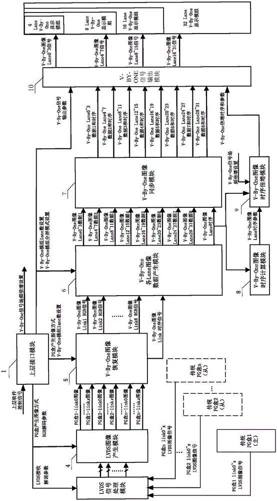
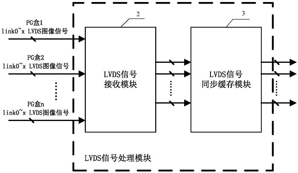
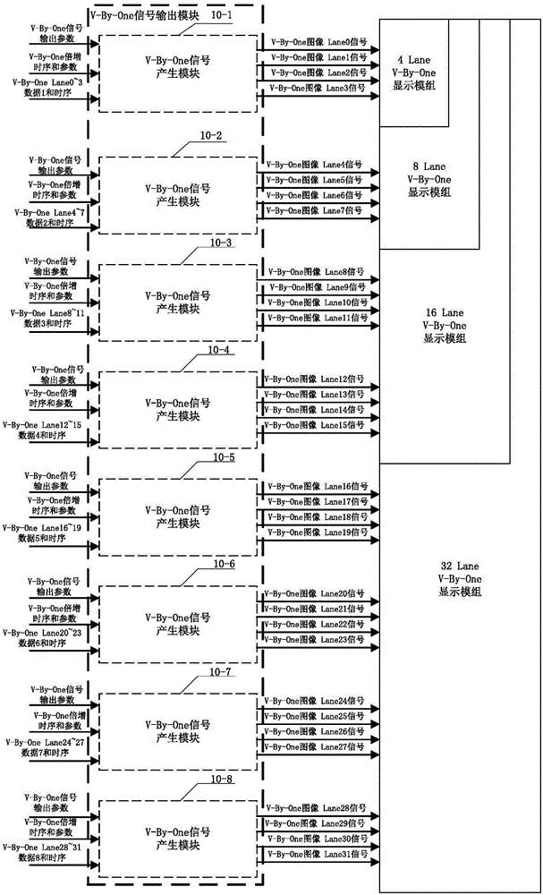
[0067] figure 1 As shown, it is a functional schematic diagram of the signal conversion device provided by the embodiment of the invention, including an upper layer interface module 1 solidified on a programmable logic device, an LVDS signal processing module, an LVDS image generation module 4, and a V-BY-ONE image recovery module. Module 5, V-BY-ONE each Lane image data generation module 6, V-BY...


PUM


Abstract

The invention discloses a signal conversion method and device. According to the method, image data partition processing and field frequency multiplication processing are carried out on a low voltage differential signaling (LVDS) with low resolution and brush frequency output from a traditional image signal source to generate a signal applicable to dot screen test of a V-BY-ONE display module, and thus, the purpose of lighting the V-BY-ONE display modules with resolution of 4k, 8k and 10k, various different display Lane numbers and display screen modes by the existing image signal source is achieved. The device provided by the invention can be used for receiving external configuration through an upper-layer interface module, can be applicable to the V-BY-ONE modules with different resolutions, also can be suitable for the LVDS image signals input from various traditional image signal sources, and has the advantages of simplicity and convenience in operation; on the other hand, the device can be implemented by a field programmable gate array (FPGA) chip, and the technical scheme is flexible; and moreover, the device has the characteristics of relatively low cost and stable working performance.

Description

technical field [0001] The invention belongs to the technical field of signal processing, and more specifically relates to a signal conversion method and device for lighting a super-high-resolution V-BY-ONE display module by using a low-resolution image signal source. Background technique [0002] With the development of liquid crystal display technology, large-size display devices with ultra-high-definition 4K resolution (3840×2160) (display area greater than 50 inches) have become popular, and large-size display devices with ultra-high-definition 8K resolution (7680×4320) have also become popular. Start mass production. In order to achieve ultra-high resolution display performance, ensure the reliability of use, and reduce manufacturing costs, these display device modules mostly use V-BY-ONE video interface technology to receive image signals. [0003] The V-BY-ONE display module is mainly tested by displaying static images. Since many manufacturers are shifting from ord...

Claims


Application Information

Patent Timeline
IPC IPC(8): H04N7/01G09G3/20G09G3/00
CPCG09G3/006G09G3/2096H04N7/012
Inventor 朱亚凡许恩沈亚非
Owner WUHAN JINGCE ELECTRONICS GRP CO LTD
Why Eureka
Try Eureka